

Ad Support : Nano Technology Netbook Technology News Computer Software
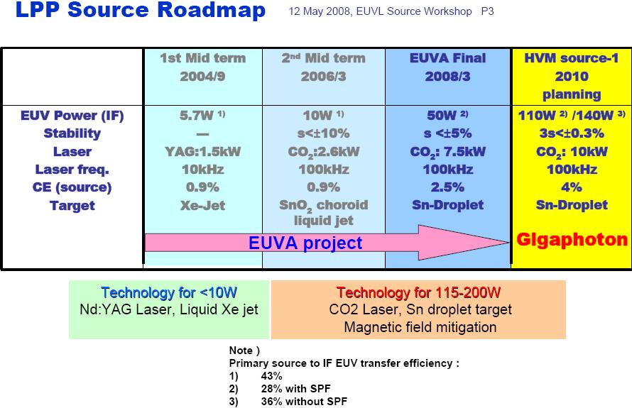
Gigaphoton (Japan) announced a 104 watt Extreme Ultraviolet (EUV) light source which is a critical part for the realization of the first volume-production-worthy EUV light source target for 2011. It was made under the Laser Produced Plasma (LPP) Light Source Development Program for EUV Lithography, it is promoted by EUVA.
* Nikon believes that > 0.35 NA optics is needed for a two-generation EUVL tool and sees EUVL being used at the 16 nm node. To extend 193 nm lithography, Ushida proposed a “line cutting” concept along with two sets of patterns on the same mask to make double patterning cost-effective
* Nikon believes that its HVM EUVL tool will need 0.4 or higher NA. During Q&A, Nikon’s Takaharu Miura pointed out the company is still working to achieve 0.4 NA with six-mirror designs in an effort to avoid an eight-mirror design, which would lose throughput because of additional reflective surfaces.
* ASML reported that NXE:3100 loses 20% of source power to dose control and will lose an additional 35% to the spectral purity filter (SPF) — thus reducing 200 W of “raw power” (i.e., measured power at IF and the current indicator of power specs for sources) to 104 W of “exposure power” (i.e., power available for printing). In other words, two new loss mechanisms were identified for source power, and it is “exposure power” that defines tool throughput.
* ASML is currently conducting acceptance testing at Cymer for a source that provides 20 W of exposure power, which corresponds to 15 wph (wafers per hour) throughput. ASML expects to get 40 W from Cymer’s source this year to improve throughput to 25 wph, and the specs for the NXE:3100 are at 100 W for a 60 wph scanner.
* ASML showed data to prove that EUVL offers twice the depth of focus (DOF) and 30% feature size reduction over 193 nm lithography. Transmission of the NXE:3100 has been doubled since alpha demonstration, and an additional 50% increase (or 3× improvement) in throughput over ADT is planned for the HVM tool. ASML’s HVM roadmap has 500 W of exposure power, and laser-produced plasma (LPP) EUV sources seem to be the only way to achieve that goal. ASML believes that EUVL is the only cost-effective technology for foundries, and noted that fab floor requirements for EUVL are 2× less than for double patterning.
Samsung, Intel, GlobalFoundries, Hynix, Toshiba and TSMC are leading the development research for EUVL. Samsung wants EUVL ready by 2012, and TSMC announced during the conference that its has ordered an NXE:3100 tool from ASML. If this tool reaches its milestone of 60 wph as planned by 2011, I can see the next improved version being able to produce 100+ wph, which can get memory makers and foundries started with EUVL in the next few years to support printing of critical layers.
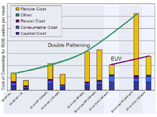
All the cost of ownership (CoO) analyses that [Vivek Baksh] has seen show EUVL to be more cost-effective than double patterning, even with mask costs taken into account
* Although 2×improvement in mask defectivity has been achieved (Fig. 4), much more must be done to reduce remaining defects
* there is EUV resist progress
AZ Electronic Materials, Sematech and Toshiba are working EUV resists.
* EUV patterning of 0.042 µm2 SRAM cells demonstrate a performance advantage over 193 nm lithography.
Here is a 22 page presentation on the Gigatron EUV lightsource work from 2008.
As previously reported Intel will use immersion lithography to the 11 nanometer node and junctionless transistors will help simplify scaling from 10 nanometers and smaller.
Gigatron 104 Watt Details
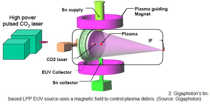
As double patterning lithography using 193-nm argon fluoride (ArF) immersion lithography tools approaches the limits of half-pitch scaling in advanced semiconductor manufacturing, an EUV light source with a shorter wavelength of 13.5 nm is considered to be an essential solution that will allow Moore’s law to be extended over the next several generations of semiconductor devices. However, one of the biggest challenges facing EUV lithography tools is the ability to achieve a higher output power, which is critical for volume production applications. Gigaphoton’s achievement in this area tackles a key hurdle and is a result of years of development work in EUV light source technology. This work has included major breakthroughs in the use of tin (Sn) targets and carbon dioxide (CO2) lasers for improved conversion efficiency, as well as the use of magnetic fields for debris removal.
Today’s announcement verifies the success of this combination of technologies. “The ability to achieve a light source output of 100 Watts will drive the cost of ownership of EUV lithography tools down to match that of double-patterning immersion lithography tools. We believe that this, in turn, will increase industry support for EUV lithography and accelerate momentum on achieving further breakthroughs in power to meet the needs for future patterning requirements,” said Dr Yuji Watanabe, president of Gigaphoton. “During this quarter, we will begin ramping operations within our state-of-the-art factory to commence initial volume production of EUV light sources with shipments slated for 2011. We are not only excited, but prepared to take advantage of the opportunities and potential afforded by EUV.”
If you liked this article, please give it a quick review on Reddit, or StumbleUpon. ThanksSupporting Advertising
Business Success
How to Make Money
Executive Jobs
Paid SurveysThank You

Brian Wang is a Futurist Thought Leader and a popular Science blogger with 1 million readers per month. His blog Nextbigfuture.com is ranked #1 Science News Blog. It covers many disruptive technology and trends including Space, Robotics, Artificial Intelligence, Medicine, Anti-aging Biotechnology, and Nanotechnology.
Known for identifying cutting edge technologies, he is currently a Co-Founder of a startup and fundraiser for high potential early-stage companies. He is the Head of Research for Allocations for deep technology investments and an Angel Investor at Space Angels.
A frequent speaker at corporations, he has been a TEDx speaker, a Singularity University speaker and guest at numerous interviews for radio and podcasts. He is open to public speaking and advising engagements.
