

Ad Support : Nano Technology Netbook Technology News Computer Software
Energy-Efficient Computing for Extreme Scale Science (10 page pdf) updates the research to making multi-petaflop and exaflop scale systems using Tensilica chips
A straw design based on 2008 Tensilica chips could theoretically achieve 200 petaflops peak with $75 million in cost and 3 megawatts of power. Next generation chips and networking available before 2015 would push the system to exaflop performance.
A many-core processor design for high-performance systems draws from embedded computing’s low-power architectures and design processes, providing a radical alternative to cluster solutions.
We have developed Green Flash, an application-driven design that combines a many-core processor with novel alternatives to cache coherence and autotuning to improve the kernels’ computational efficiency. This approach can achieve two-orders-of magnitude improvement in computational efficiency for climate simulation relative to a conventional symmetric multiprocessor (SMP) approach.
We originally estimated 10 petaflops as the sustained computational rate necessary to simulate Earth’s climate 1,000 times faster than it actually occurs. An updated estimate of the requirements for the CSU model raised that to as high as 70 petaflops—an example of the considerable uncertainty in making these estimates.
Peter Ungaro, CEO of Cray Computing, recently remarked that “Our current technologies can get us to the 10-20 petaflops range. But then to start to think about 100 [petaflops], we really need a major shift in technology.”
The proposed Tensilica exaflop system would use 20 million energy efficient Tensilica CPUs.
In our search for a radical alternative, we turned to the embedded-processor market, which successfully addresses the custom and cost issues. The industry relies on sophisticated tool chains that enable the rapid and cost-effective turnaround of power-efficient semicustom design implementations appropriate to each application.
Our design, Green Flash, leverages the same tool chains to design power-efficient exascale systems, tailoring embedded chips to target scientific applications. Rather than ask, What kind of scientific applications can run on our high-performance computing cluster? after it arrives, we have turned the question around to ask, What kind of system should be built to meet the needs of the most important science problems? This approach lets us realize the most substantial gains in energy efficiency because we essentially peel back the complexity of a high-frequency microprocessor design point to reduce waste—wasted opcodes, wasted bandwidth, waste caused by orienting architectures toward serial performance. We also change the notion of commodity from that of component-level integration of clusters to integration of commodity circuit designs within a chip for a system-on-chip.
By using hardware-software cotuning, our design enables rapid hardware design and establishes a feedback path from application programmer to hardware designer. By combining an autotuning environment for software optimization with an emulation platform based on an FPGA, we can simultaneously develop software optimizations and a semispecialized processor design. Essentially, we have not only built on proven ideas, but we have taken them in a new direction.
Here is a link to the Scidac Review of the Green Flash Design
Power efficiency requires reducing the power consumption of all system components. With these highly efficient tiny processing elements there is a danger that communication bottlenecks—both in energy and time—will result in a less efficient overall system. To mitigate this danger, long-term research requires exploring interconnect architectures that will both increase performance and reduce energy use.
One promising approach is to combine 3D CMOS integration with research into silicon photonics to build hybrid electronic-photonic interconnects on-chip. Designers place photonic detectors and emitters along with specialized low-power photonic switching elements on a special interconnect layer and interface them with processing elements using conventional electronic routers. Figure A shows how the switching elements work. Large-scale communications occur over photonic links, which have several strong advantages over electronic networks. Energy consumption for photonics is less dependent on signaling rate and distance compared to electronics, and the photonic switches are much simpler as they do not require buffers or repeaters.
Preliminary research with messaging patterns arising from scientific
applications shows that such hybrid networks have the potential to bring major gains in efficiency, due to their lower power consumption combined with fast propagation speed. Early research studies done in collaboration with the Lightwave Research Laboratory at Columbia University, for example, show that a hybrid electronic-photonic interconnect composed of ring resonators can deliver 27x better energy efficiency than electrical interconnects alone.
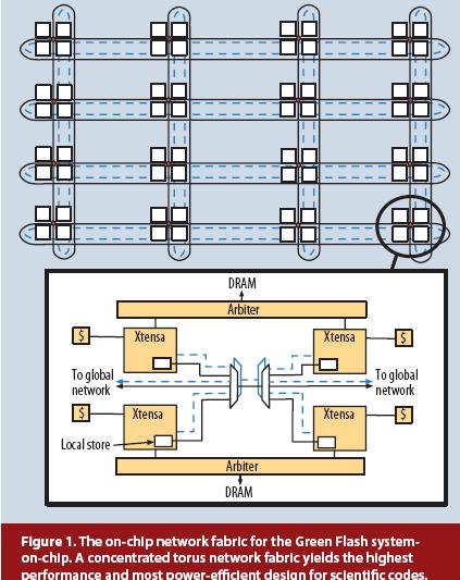
Green Flash Design
Green Flash represents a radical approach that breaks through the slow pace of incremental change. It demonstrates
that application-driven computing design can foster a sustainable hardware-software ecosystem with broad-based support across the IT industry. In evolving Green Flash, we explored practical advanced programming
models together with lightweight hardware support mechanisms that allow programmers to use massive on-chip concurrency.
Green Flash has provided insights into how designers can evolve massively parallel chip architectures through a feedback path that closely couples application, algorithm, and hardware design. Application-driven design ensures that hardware design is not driven by reactions to hardware
constraints—reactions that ignore programmability and delivered application performance. Our exploration of the climate model allowed us to investigate questions that cut across all application areas and have ramifications for the next generation of fully general-purpose architectures. Ultimately, we envision an architecture that can exploit reusable components from the mass embedded computing market while improving programmability for a many-core design. The future building blocks of a high-performance computing system will serve the performance and programmability needs of the smallest high-performance, energy-efficient embedded system all the way to extreme-scale machines
FURTHER READING
Green Flash page at Berkeley Labs
If you liked this article, please give it a quick review on Reddit, or StumbleUpon. Thanks
Supporting Advertising
Business Success
How to Make Money
Executive Jobs
Paid Surveys
Thank You

Brian Wang is a Futurist Thought Leader and a popular Science blogger with 1 million readers per month. His blog Nextbigfuture.com is ranked #1 Science News Blog. It covers many disruptive technology and trends including Space, Robotics, Artificial Intelligence, Medicine, Anti-aging Biotechnology, and Nanotechnology.
Known for identifying cutting edge technologies, he is currently a Co-Founder of a startup and fundraiser for high potential early-stage companies. He is the Head of Research for Allocations for deep technology investments and an Angel Investor at Space Angels.
A frequent speaker at corporations, he has been a TEDx speaker, a Singularity University speaker and guest at numerous interviews for radio and podcasts. He is open to public speaking and advising engagements.