

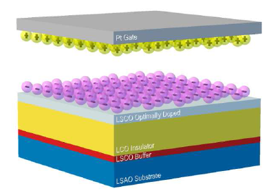
Schematics of a typical LSCO-LCO heterostructure used to fabricate EDLT devices. For clarity, the polymer electrolyte (or the ionic liquid) is not shown; we just show the anions adsorbed to the film surface and the cations attracted to the negatively charged Pt gate electrode.
Like atomic-level bricklayers, researchers from the U.S. Department of Energy’s (DOE) Brookhaven National Laboratory are using a precise atom-by-atom layering technique to fabricate an ultrathin transistor-like field effect device to study the conditions that turn insulating materials into high-temperature superconductors. The technical break-through, which is described in the April 28, 2011, issue of Nature, is already leading to advances in understanding high-temperature superconductivity, and could also accelerate the development of resistance-free electronic devices
Nature – Superconductor–insulator transition in La2 − xSrxCuO4 at the pair quantum resistance

Schematics of a HTS electrolyte double-layer transistor (HTS-EDLT) device with a coplanar gate electrode. The film contains a about 1 nm thick LSCO layer on top of an insulating LCO layer (typically 3-5 nm thick). Ten contacts allow for longitudinal and Hall resistance measurements. A larger area coplanar gate electrode allows for field focusing. Ionic liquid or polymer electrolyte covers and connects the gate electrode with the Hall bar. For a negative gate voltage, cations (DEME+ or Na+) are drawn to the gate and anions (TFSI- or F-) to the HTS film surface, respectively.
“Understanding exactly what happens when a normally insulating copper-oxide material transitions from the insulating to the superconducting state is one of the great mysteries of modern physics,” said Brookhaven physicist Ivan Bozovic, lead author on the study.
One way to explore the transition is to apply an external electric field to increase or decrease the level of “doping” — that is, the concentration of mobile electrons in the material — and see how this affects the ability of the material to carry current. But to do this in copper-oxide (cuprate) superconductors, one needs extremely thin films of perfectly uniform composition — and electric fields measuring more than 10 billion volts per meter. (For comparison, the electric field directly under a power transmission line is 10 thousand volts per meter.)
Bozovic’s group has employed a technique called molecular beam epitaxy (MBE) to uniquely create such perfect superconducting thin films one atomic layer at a time, with precise control of each layer’s thickness. Recently, they’ve shown that in such MBE-created films even a single cuprate layer can exhibit undiminished high-temperature superconductivity.*
Now, they’ve applied the same technique to build ultrathin superconducting field effect devices that allow them to achieve the charge separation, and thus electric field strength, for these critical studies.
These devices are similar to the field-effect transistors (FETs) that are the basis of all modern electronics, in which a semiconducting material transports electrical current from the “source” electrode on one end of the device to a “drain” electrode on the other end. FETs are controlled by a third electrode, called a “gate,” positioned above the source-drain channel — separated by a thin insulator — which switches the device on or off when a particular gate voltage is applied to it.
But because no known insulator could withstand the high fields required to induce superconductivity in the cuprates, the standard FET scheme doesn’t work for high-temperature superconductor FETs. Instead, the scientists used electrolytes, liquids that conduct electricity, to separate the charges.
In this setup, when an external voltage is applied, the electrolyte’s positively charged ions travel to the negative electrode and the negatively charged ions travel to the positive electrode. But when the ions reach the electrodes, they abruptly stop, as though they’ve hit a brick wall. The electrode “walls” carry an equal amount of opposite charge, and the electric field between these two oppositely charged layers can exceed the 10 billion volts per meter goal.
The result is a field effect device in which the critical temperature of a prototype high-temperature superconductor compound (lanthanum-strontium-copper-oxide) can be tuned by as much as 30 degrees Kelvin, which is about 80 percent of its maximal value — almost ten times more than the previous record.
The scientists have now used this enhanced device to study some of the basic physics of high-temperature superconductivity.
One key finding: As the density of mobile charge carriers is increased, their cuprate film transitions from insulating to superconducting behavior when the film sheet resistance reaches 6.45 kilo-ohm. This is exactly equal to the Planck quantum constant divided by twice the electron charge squared — h/(2e)2. Both the Planck constant and electron charge are “atomic” units — the minimum possible quantum of action and of electric charge, respectively, established after the advent of quantum mechanics early in the last century.
“It is striking to see a signature of such clearly quantum-mechanical behavior in a macroscopic sample (up to millimeter scale) and at a relatively high temperature,” Bozovic said. Most people associate quantum mechanics with characteristic behavior of atoms and molecules.
This result also carries another surprising message. While it has been known for many years that electrons are paired in the superconducting state, the findings imply that they also form pairs (although localized and immobile) in the insulating state, unlike in any other known material. That sets the scientists on a more focused search for what gets these immobilized pairs moving when the transition to superconductivity occurs.
Superconducting FETs might also have direct practical applications. Semiconductor-based FETs are power-hungry, particularly when packed very densely to increase their speed. In contrast, superconductors operate with no resistance or energy loss. Here, the atomically thin layer construction is in fact advantageous — it enhances the ability to control superconductivity using an external electric field.
“This is just the beginning,” Bozovic said. “We still have so much to learn about high-temperature superconductors. But as we continue to explore these mysteries, we are also striving to make ultrafast and power-saving superconducting electronics a reality.”
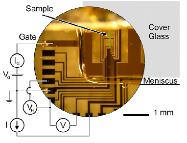
Optical micrograph of a fabricated device. The measurement circuit is indicated. The electrolyte was held in place with a glass cover slip. The gate electrode and the Hall bar are in false colours for better contrast.
High-temperature superconductivity in copper oxides arises when a parent insulator compound is doped beyond some critical concentration; what exactly happens at this superconductor–insulator transition is a key open question. The cleanest approach is to tune the carrier density using the electric field effect for example, it was learned in this way that weak electron localization transforms superconducting SrTiO3 into a Fermi-glass insulator. But in the copper oxides this has been a long-standing technical challenge, because perfect ultrathin films and huge local fields ( greater than 10^9 V m−1) are needed. Recently, such fields have been obtained using electrolytes or ionic liquids in the electric double-layer transistor configuration. Here we report synthesis of epitaxial films of La2− xSrxCuO4 that are one unit cell thick, and fabrication of double-layer transistors. Very large fields and induced changes in surface carrier density enable shifts in the critical temperature by up to 30 K. Hundreds of resistance versus temperature and carrier density curves were recorded and shown to collapse onto a single function, as predicted for a two-dimensional superconductor–insulator transition. The observed critical resistance is precisely the quantum resistance for pairs, RQ = h/(2e)2 = 6.45 kΩ, suggestive of a phase transition driven by quantum phase fluctuations, and Cooper pair (de)localization
13 pages of supplemental information
If you liked this article, please give it a quick review on ycombinator or StumbleUpon. Thanks

Brian Wang is a Futurist Thought Leader and a popular Science blogger with 1 million readers per month. His blog Nextbigfuture.com is ranked #1 Science News Blog. It covers many disruptive technology and trends including Space, Robotics, Artificial Intelligence, Medicine, Anti-aging Biotechnology, and Nanotechnology.
Known for identifying cutting edge technologies, he is currently a Co-Founder of a startup and fundraiser for high potential early-stage companies. He is the Head of Research for Allocations for deep technology investments and an Angel Investor at Space Angels.
A frequent speaker at corporations, he has been a TEDx speaker, a Singularity University speaker and guest at numerous interviews for radio and podcasts. He is open to public speaking and advising engagements.