

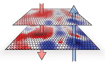
NIST measurements show that interactions of the graphene layers with the insulating substrate material causes electrons (red, down arrow) and electron holes (blue, up arrow) to collect in “puddles”. The differing charge densities creates the random pattern of alternating dipoles and electon band gaps that vary across the layers. Credit: NIST
Researchers at the National Institute of Standards and Technology (NIST) have shown that the electronic properties of two layers of graphene vary on the nanometer scale. The surprising new results reveal that not only does the difference in the strength of the electric charges between the two layers vary across the layers, but they also actually reverse in sign to create randomly distributed puddles of alternating positive and negative charges. Reported in Nature Physics,* the new measurements bring graphene a step closer to being used in practical electronic devices.
Arxiv – Microscopic Polarization in Bilayer Graphene (26 pages)
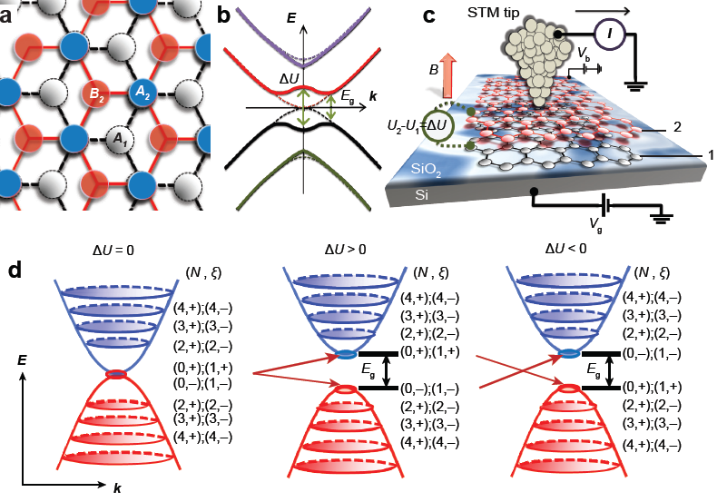
Schematics of the bilayer graphene measurements and energy band diagram in the
quantum Hall regime. a, Schematic of Bernal-stacked bilayer graphene consisting of a top layer (A2/B2) and bottom layer (A1/B1), with atom A2 directly over B1. b, Energy band diagram of bilayer graphene with (solid lines) and without (dashed lines) a band gap. The electronic levels form Mexican-hat like energy bands with a potential energy asymmetry ΔU and a band gap of Eg. c, Schematic of a gated bilayer graphene device for STM/STS measurement with circuitry showing application of gate voltage Vg and sample bias Vb. The bilayer graphene is placed on a 300 nm SiO2 substrate separating from a back gate electrode (Si). The disorder potential induced from the substrate is illustrated in color overlaid on the SiO2 surface. ΔU equals to the difference between onsite energies for the top (2) and the bottom (1) layers. Magnetic field B is perpendicular to the sample plane. d, The formation of bilayer graphene Landau levels in the quantum Hall regime with and without a band gap. Landau levels are indexed with the orbital and valley index, (N , ξ), and each is two-fold degenerate in spin. The eight-fold degenerate N = 0, 1 levels become layer polarized quartets when the graphene layers are subjected to a potential energy asymmetry ΔU. LL(0,+);(1,+) projected on the top layer (ξ = +1) depends on the sign of ΔU.M
Graphene, a single layer of carbon atoms, is prized for its remarkable properties, not the least of which is the way it conducts electrons at high speed. However, the lack of what physicists call a band gap—an energetic threshold that makes it possible to turn a transistor on and off—makes graphene ill-suited for digital electronic applications.
Researchers have known that bilayer graphene, consisting of two stacked graphene layers, acts more like a semiconductor when immersed in an electric field.
According to NIST researcher Nikolai Zhitenev, the band gap may also form on its own due to variations in the sheets’ electrical potential caused by interactions among the graphene electrons or with the substrate (usually a nonconducting, or insulating material) that the graphene is placed upon.
NIST fellow Joseph Stroscio says that their measurements indicate that interactions with the disordered insulating substrate material causes pools of electrons and electron holes (basically, the absence of electrons) to form in the graphene layers. Both electron and hole “pools” are deeper on the bottom layer because it is closer to the substrate. This difference in “pool” depths, or charge density, between the layers creates the random pattern of alternating charges and the spatially varying band gap.
Manipulating the purity of the substrate could give researchers a way to finely control graphene’s band gap and may eventually lead to the fabrication of graphene-based transistors that can be turned on and off like a semiconductor.
Still, as shown in the group’s previous work**, while these substrate interactions open the door to graphene’s use as a practical electronic material, they lower the window on speed. Electrons do not move as well through substrate-mounted bilayer graphene; however, this may likely be compensated for by engineering the graphene/substrate interactions.
Stroscio’s team plans to explore further the role that substrates may play in the creation and control of band gaps in graphene by using different substrate materials. If the substrate interactions can be reduced far enough, says Stroscio, the exotic quantum properties of bilayer graphene may be harnessed to create a new quantum field effect transistor.
Bilayer graphene has drawn significant attention due to the opening of a band gap in its low energy electronic spectrum, which offers a promising route to electronic applications. The gap can be either tunable through an external electric field or spontaneously formed through an interaction-induced symmetry breaking. Our scanning tunneling measurements reveal the microscopic nature of the bilayer gap to be very different from what is observed in previous macroscopic measurements or expected from current theoretical models. The potential difference between the layers, which is proportional to charge imbalance and determines the gap value, shows strong dependence on the disorder potential, varying spatially in both magnitude and sign on a microscopic level. Furthermore, the gap does not vanish at small charge densities. Additional interaction-induced effects are observed in a magnetic field with the opening of a subgap when the zero orbital Landau level is placed at the Fermi energy.
If you liked this article, please give it a quick review on ycombinator or StumbleUpon. Thanks

Brian Wang is a Futurist Thought Leader and a popular Science blogger with 1 million readers per month. His blog Nextbigfuture.com is ranked #1 Science News Blog. It covers many disruptive technology and trends including Space, Robotics, Artificial Intelligence, Medicine, Anti-aging Biotechnology, and Nanotechnology.
Known for identifying cutting edge technologies, he is currently a Co-Founder of a startup and fundraiser for high potential early-stage companies. He is the Head of Research for Allocations for deep technology investments and an Angel Investor at Space Angels.
A frequent speaker at corporations, he has been a TEDx speaker, a Singularity University speaker and guest at numerous interviews for radio and podcasts. He is open to public speaking and advising engagements.