
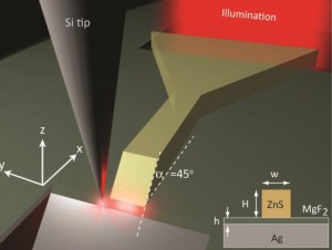

The hybrid plasmon polariton (HPP) nanoscale waveguide consists of a semiconductor strip separated from a metallic surface by a low dielectric gap. Schematic shows HPP waveguide responding when a metal slit at the guide’s input end is illuminated. (courtesy of Zhang group)
The creation of a new quasiparticle called the “hybrid plasmon polariton” may throw open the doors to integrated photonic circuits and optical computing for the 21st century. Researchers with the U.S. Department of Energy (DOE)’s Lawrence Berkeley National Laboratory (Berkeley Lab) have demonstrated the first true nanoscale waveguides for next generation on-chip optical communication systems.

Emerging communication applications call for a road map towards nanoscale photonic components and systems. Although metal-based nanostructures theoretically offer a solution to enable nanoscale photonics, the key demonstration of optical modes with deep sub-diffraction-limited confinement and significant propagation distances has not been experimentally achieved because of the trade-off between optical confinement and metallic losses. Here we report the first experimental demonstration of truly nanoscale guided waves in a metal– insulator–semiconductor device featuring low-loss and broadband operation. Near-field scanning optical microscopy reveals mode sizes down to 50×60 nm2 at visible and near-infrared wavelengths propagating more than 20 times the vacuum wavelength. Interference spectroscopy confirms that the optical mode hybridization between a surface plasmon and a dielectric mode concentrates the hybridized mode inside a nanometre thin gap. This nanoscale waveguide holds promise for next generation on-chip optical communication systems that integrate light sources, modulators or switches, nonlinear and quantum optics.
“We have directly demonstrated the nanoscale waveguiding of light at visible and near infrared frequencies in a metal-insulator-semiconductor device featuring low loss and broadband operation,” says Xiang Zhang, the leader of this research. “The novel mode design of our nanoscale waveguide holds great potential for nanoscale photonic applications, such as intra-chip optical communication, signal modulation, nanoscale lasers and bio-medical sensing.”
Zhang and his co-authors describe the use of the hybrid plasmon polariton, a quasi-particle they conceptualized and created, in a nanoscale waveguide system that is capable of shepherding light waves along a metal-dielectric nanostructure interface over sufficient distances for the routing of optical communication signals in photonic devices. The key is the insertion of a thin low-dielectric layer between the metal and a semiconductor strip.
“We reveal mode sizes down to 50-by-60 square nanometers using Near-field scanning optical microscopy (NSOM) at optical wavelengths,” says Volker Sorger a graduate student in Zhang’s research group and one of the two lead authors on the Nature Communications paper. “The propagation lengths were 10 times the vacuum wavelength of visible light and 20 times that of near infrared.”
“Until now, the direct experimental demonstration of low-loss propagation of deep sub-wavelength optical modes was not realized due to the huge propagation loss in the optical mode that resulted from the electromagnetic field being pushed into the metal,” Zhang says. “With this trade-off between optical confinement and metallic losses, the use of plasmonics for integrated photonics, in particular for optical interconnects, has remained uncertain.”
To solve the problem of optical signal loss, Zhang and his group proposed the hybrid plasmon polariton (HPP) concept. A semiconductor (high-dielectric) strip is placed on a metal interface, just barely separated by a thin oxide (low-dielectric) layer. This new metal-oxide-semiconductor design results in a redistribution of an incoming light wave’s energy. Instead of being concentrated in the metal, where optical losses are high, some of the light wave’s energy is squeezed into the low dielectric gap where optical losses are substantially less compared to the plasmonic metal.
“With this design, we create an HPP mode, a hybrid of the photonic and plasmonic modes that takes the best from both systems and gives us high confinement with low signal loss,” says Ziliang Ye, the other lead authors of the Nature Communications paper who is also a graduate student in Zhang’s research group. “The HPP mode is not only advantageous for down-scaling physical device sizes, but also for delivering novel physical effects at the device level that pave the way for nanolasers, as well as for quantum photonics and single-photon all-optical switches.”
The HPP waveguide system is fully compatible with current semiconductor/CMOS processing techniques, as well as with the Silicon-on-Insulator (SOI) platform used today for photonic integration. This should make it easier to incorporate the technology into low-cost, large-scale integration and manufacturing schemes. Sorger believes that prototypes based on this technology could be ready within the next two years and the first actual products could be on the market within five years.
“We are already working on demonstrating an all-optical transistor and electro-optical modulator based on the HPP waveguide system,” Sorger says. “We’re also now looking into bio-medical applications, such as using the HPP waveguide to make a molecular sensor.”
6 pages of supplemental information
If you liked this article, please give it a quick review on ycombinator or StumbleUpon. Thanks

Brian Wang is a Futurist Thought Leader and a popular Science blogger with 1 million readers per month. His blog Nextbigfuture.com is ranked #1 Science News Blog. It covers many disruptive technology and trends including Space, Robotics, Artificial Intelligence, Medicine, Anti-aging Biotechnology, and Nanotechnology.
Known for identifying cutting edge technologies, he is currently a Co-Founder of a startup and fundraiser for high potential early-stage companies. He is the Head of Research for Allocations for deep technology investments and an Angel Investor at Space Angels.
A frequent speaker at corporations, he has been a TEDx speaker, a Singularity University speaker and guest at numerous interviews for radio and podcasts. He is open to public speaking and advising engagements.