
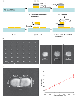

Device fabrication. a) Schematic diagram of fabrication process. b) SEM image of a fabricated dimer array obtained with 50k × magnifi cation.
c) SEM image of a dimer structure in the fabricated array of (b) obtained with 420k × magnifi cation. d–f) SEM images of the left side of the dimer
structure, after ambient oxidation (d), 2 min oxygen plasma (e), and pattern without silver/chromium layer for comparison, which is taken by
etching the left-side pattern with chromium etchant just after the oxidation process (f). g) Gap size, determined from SEM, as a function of oxygen
plasma time. Each error bar represents standard deviation of gap size for a particular dimer array, determined from nine randomly selected dimers
within the array.
Small Journal – Lithographically Fabricated Optical Antennas with Gaps Well Below 10 nm (6 pages)
In this work, we demonstrate arrays of dimers with controllable gap size well below 10 nm by combining electron beam lithography with the use of sacrificial layers. The measured SERS enhancement factors increase almost by two orders of magnitude by reducing the gap size from ≈ 20 nm to ≈ 3 nm. This significant improvement confirms that there is a substantial electromagnetic field generated within dimer gaps.
Metal nanostructures that efficiently capture or radiate electromagnetic waves at optical frequencies offer a means to concentrate electromagnetic energy into deep subwavelength regions. Wessel noted that these structures can therefore be considered antennas. Recent work has focused on more efficient designs, termed ‘optical antennas’, which employ small gaps or very sharp tips. Optical antennas present opportunities for ultrasensitive spectroscopy, near-field scanning optical microscopy, and compact subwavelength light sources. However, the achievable feature sizes are usually determined by fabrication, being approximately given by the gap size or tip sharpness. Here, we report a top-down fabrication procedure to fabricate pairs of nanoparticles separated by a controllable gap size that can be as small as 3 nm. As an application, we show that the enhancement factors of surface enhanced Raman scattering (SERS) increase significantly for smaller gap sizes, indicating greatly enhanced electromagnetic fields within the gaps. We anticipate that the fabrication method we introduce here for nanoparticle pairs with nanoscale gaps would be useful not only for SERS, where it could potentially enable single-molecule sensitivity, but also for other applications in plasmonics.
In conclusion, we have developed a fabrication procedure based on a sacrificial layer for the lithographic fabrication of optical antennas with gaps well below 10 nm. We demonstrate that the gap size can be effectively controlled by oxidizing the sacrificial layer using oxygen plasma. Localized electromagnetic fields can be significantly enhanced within the nanoscale gaps, as indicated by SERS measurements. This work enhances the ability to fabricate reproducible SERS substrates using a top-down method with a high enhancement factor. Moreover, by offering an accessible approach to fabricate features well below 10 nm, we anticipate that this technique will enable the fabrication of novel plasmonic structures otherwise not possible with standard techniques.
9 pages of supplemental information
List of publications by the Crozier group at Harvard
If you liked this article, please give it a quick review on ycombinator or StumbleUpon. Thanks

Brian Wang is a Futurist Thought Leader and a popular Science blogger with 1 million readers per month. His blog Nextbigfuture.com is ranked #1 Science News Blog. It covers many disruptive technology and trends including Space, Robotics, Artificial Intelligence, Medicine, Anti-aging Biotechnology, and Nanotechnology.
Known for identifying cutting edge technologies, he is currently a Co-Founder of a startup and fundraiser for high potential early-stage companies. He is the Head of Research for Allocations for deep technology investments and an Angel Investor at Space Angels.
A frequent speaker at corporations, he has been a TEDx speaker, a Singularity University speaker and guest at numerous interviews for radio and podcasts. He is open to public speaking and advising engagements.