
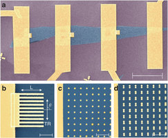

Scanning electron microscopy micrographs of the graphene devices with plasmonic nanostructures.
In the new research, the team combined graphene with metallic nanostructures, leading to a twenty-fold enhancement in the harvesting of light to create energy. This paves the way for future advances in high-speed internet development and other communications.
Nature Communications – Strong plasmonic enhancement of photovoltage in graphene
From the wide spectrum of potential applications of graphene, ranging from transistors and chemical sensors to nanoelectromechanical devices and composites, the field of photonics and optoelectronics is believed to be one of the most promising. Indeed, graphene’s suitability for high-speed photodetection was demonstrated in an optical communication link operating at 10 Gbit per second. However, the low responsivity of graphene-based photodetectors compared with traditional III–V-based ones is a potential drawback. Here we show that, by combining graphene with plasmonic nanostructures, the efficiency of graphene-based photodetectors can be increased by up to 20 times, because of efficient field concentration in the area of a p–n junction. Additionally, wavelength and polarization selectivity can be achieved by employing nanostructures of different geometries.
Previous studies had already shown how graphene can be used to create an elementary solar cell. If two closely-spaced metallic wires are put on top of graphene and light is shone on the structure, it generates an electric voltage.
The major stumbling block towards practical applications for these otherwise very promising devices has so far been their low efficiency, however. The problem is that graphene – the thinnest material in the world – absorbs little light (approximately just 3%), while the rest goes through it without contributing to electrical power.
The Cambridge and Manchester team solved the problems by combining graphene with tiny metallic structures which are arranged on top of it. These so-called plasmonic nanostructures have dramatically enhanced the optical electric field felt by graphene and effectively concentrated light within the one-atom-thick carbon layer.
By using the plasmonic enhancement, the light-harvesting performance of graphene was boosted 20 times over, without sacrificing any of its speed. In future, the efficiency of graphene in this regard will be improved even further.
Professor Andrea Ferrari, from the Cambridge Engineering Department, who led the Cambridge effort in the collaboration, said: “So far, the main focus of graphene research has been on fundamental physics and electronic devices.”
“These results show its great potential in the fields of photonics and optoelectronics, where the combination of its unique optical and electronic properties with plasmonic nanostructures can be fully exploited, even in the absence of a bandgap, in a variety of useful devices, such as solar cells and photodetectors.”
Professor Novoselov, from the Manchester team, added: “The technology of graphene production matures day by day, which has an immediate impact both on the type of exciting physics which we find in this material, and on the feasibility and the range of possible applications.”
“Many leading electronics companies consider graphene for the next generation of devices. This work certainly boosts graphene’s chances even further.”
If you liked this article, please give it a quick review on ycombinator or StumbleUpon. Thanks

Brian Wang is a Futurist Thought Leader and a popular Science blogger with 1 million readers per month. His blog Nextbigfuture.com is ranked #1 Science News Blog. It covers many disruptive technology and trends including Space, Robotics, Artificial Intelligence, Medicine, Anti-aging Biotechnology, and Nanotechnology.
Known for identifying cutting edge technologies, he is currently a Co-Founder of a startup and fundraiser for high potential early-stage companies. He is the Head of Research for Allocations for deep technology investments and an Angel Investor at Space Angels.
A frequent speaker at corporations, he has been a TEDx speaker, a Singularity University speaker and guest at numerous interviews for radio and podcasts. He is open to public speaking and advising engagements.