

Researchers have invented a tiny Etch-A-Sketch® that draws infinitesimally small “wires” on a surface, then erases them. The device works by switching an oxide crystal between insulating and conducting states. The interface between these two materials can be switched between an insulating and metallic state using a sharp conducting probe. Electronic circuits can be “written” and “erased” at scales approaching the distance between atoms (two nanometers). The device, less than four nanometers wide, enables photonic interaction with objects as small as single molecules or quantum dots.
Beyond being just plain cool, this device could be the basis of an entirely new kind of transistor.
Transistors in a computer are the on/off switches that enable the efficient implementation of complex computational systems. And for the last half century, they’ve been getting smaller and smaller, according to (Intel founder Gordon) “Moore’s law”: The number of transistors that can be placed inexpensively on an integrated circuit doubles approximately every two years. At some point, though, this trend has to stop. Materials start acting “weird” when they are made too small. The useful properties of silicon, for example, are believed to break down at distances smaller than 10 nanometers.
“The question is, once you’ve pushed silicon to its limit, is there going to be another system to do computation?” asks Levy. That’s really what we’ve been granted funding to explore. We’re trying to break down the major barriers that are potential show-stoppers that would otherwise make it difficult to turn these new types of devices into real, useful things.”
Nature Nanotechnology – Sketched oxide single-electron transistor
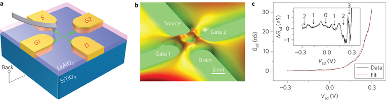
SketchSET schematic and transport characteristics.
Devices that confine and process single electrons represent an important scaling limit of electronics. Such devices have been realized in a variety of materials and exhibit remarkable electronic, optical and spintronic properties. Here, we use an atomic force microscope tip to reversibly ‘sketch’ single-electron transistors by controlling a metal–insulator transition at the interface of two oxides. In these devices, single electrons tunnel resonantly between source and drain electrodes through a conducting oxide island with a diameter of ~1.5 nm. We demonstrate control over the number of electrons on the island using bottom- and side-gate electrodes, and observe hysteresis in electron occupation that is attributed to ferroelectricity within the oxide heterostructure. These single-electron devices may find use as ultradense non-volatile memories, nanoscale hybrid piezoelectric and charge sensors, as well as building blocks in quantum information processing and simulation platforms.
How today’s computers process information depends on a fixed architecture of ones and zeros—digital logic. Levy envisions using new materials that might not follow that same architecture. “We want the material to tell us the best way it can do computation, rather than trying to impose an old architecture that was really designed for another type of material,” he says. “We want to listen to the material, and then map information processing onto what it’s good at.”
Professors Mark Rzchowski and Jack Ma at the University of Wisconsin will focus on this issue. The materials will be working with are part of a family known as “complex oxides”. This class of materials shares many of the semiconducting properties of silicon, but have a wealth of other properties that make them interesting for computing, storage and sensing applications.
All computers require storage, but they store this information using very different architectures than the computer parts. In addition, an important function of electronics is that semiconductors can be used for sensing – which in this case really means sensing of light.
“We want to try to integrate all of these things together and have a platform that allows us to ‘write’ or ‘erase’ components capable of all of these functions,” Levy says.
The principal material they wish to study is a sandwich of two such oxides: a thick layer of strontium titanate, with a thin (1.2 nanometer) layer of lanthanum aluminate. These materials will be grown in the laboratory of Professor Chang-Beom Eom at the University of Wisconsin.
Another issue Levy is studying is the amount of power that is consumed by devices as they get smaller. With laptops, for example, clock speed—processor speed—used to be everything. But now, it’s not touted as much. “Of course, that’s because manufacturers can’t make it go faster,” Levy points out. “They could increase the clock speed, but it would melt the silicon.”
7 pages of supplemental information
If you liked this article, please give it a quick review on ycombinator or StumbleUpon. Thanks

Brian Wang is a Futurist Thought Leader and a popular Science blogger with 1 million readers per month. His blog Nextbigfuture.com is ranked #1 Science News Blog. It covers many disruptive technology and trends including Space, Robotics, Artificial Intelligence, Medicine, Anti-aging Biotechnology, and Nanotechnology.
Known for identifying cutting edge technologies, he is currently a Co-Founder of a startup and fundraiser for high potential early-stage companies. He is the Head of Research for Allocations for deep technology investments and an Angel Investor at Space Angels.
A frequent speaker at corporations, he has been a TEDx speaker, a Singularity University speaker and guest at numerous interviews for radio and podcasts. He is open to public speaking and advising engagements.