

Researchers at Rensselaer Polytechnic Institute developed a new method for creating a layer of gold nanoparticles that measures only billionths of a meter thick. These self-assembling gold coatings with features measuring less than 10 nanometers could hold important implications for nanoelectronics manufacturing. This new discovery could offer new solutions for scaling down the features of today’s most advanced 32-nm computer chips to have features in the range of less than 20 nanometers, or even less than 10 nanometers.
They observed a superlattice measuring 20 microns, with a distance between lines of nanoparticles — or lattice constant — of 8.8 nanometers. He said the 20-micron superlattice domain is the largest ever documented, and this new technique could lead to even larger superlattices with even tinier features.
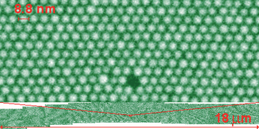
We report a very large 2D superlattice domain of hexagonal close-packed monodisperse gold nanoparticles, which is longer than 20 μm and of 8.8 nm superlattice constant in a millimetre-scale monolayer film, fabricated by simple self-assembly of drying water and toluene droplets with 2D nanoparticles at the air–liquid interfaces.
If you liked this article, please give it a quick review on ycombinator or StumbleUpon. Thanks

Brian Wang is a Futurist Thought Leader and a popular Science blogger with 1 million readers per month. His blog Nextbigfuture.com is ranked #1 Science News Blog. It covers many disruptive technology and trends including Space, Robotics, Artificial Intelligence, Medicine, Anti-aging Biotechnology, and Nanotechnology.
Known for identifying cutting edge technologies, he is currently a Co-Founder of a startup and fundraiser for high potential early-stage companies. He is the Head of Research for Allocations for deep technology investments and an Angel Investor at Space Angels.
A frequent speaker at corporations, he has been a TEDx speaker, a Singularity University speaker and guest at numerous interviews for radio and podcasts. He is open to public speaking and advising engagements.