
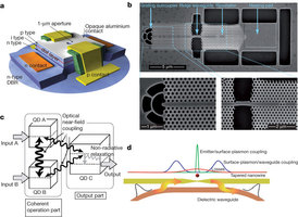
Nature – The assembly of hybrid nanophotonic devices from different fundamental photonic entities—such as single molecules, nanocrystals, semiconductor quantum dots, nanowires and metal nanoparticles—can yield functionalities that exceed those of the individual subunits. Combining these photonic elements requires nanometre-scale fabrication precision and potentially involves a material diversity that is incompatible with standard nanotechnological processes. Although merging these different systems on a single hybrid platform is at present challenging, it promises improved performance and novel devices. Particularly rapid progress is seen in the combination of plasmonic–dielectric constituents with quantum emitters that can be assembled on demand into fundamental model systems for future optical elements.

Nanophotonic functional elements.
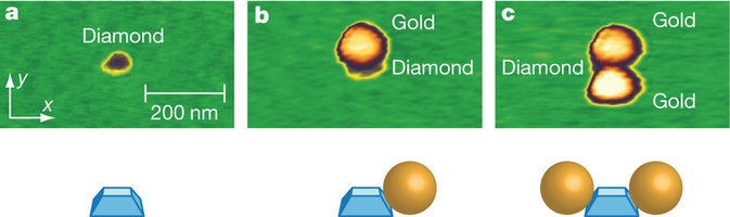
Stepwise AFM nanoassembly of a plasmonic nanoantenna. a–c, A single nitrogen–vacancy defect centre in a diamond nanocrystal (a) is sandwiched between two gold nanoparticles (60 nm in diameter) (b, c). The sketches (bottom) illustrate the configuration mapped by false-colour AFM imaging (top)
If you liked this article, please give it a quick review on ycombinator or StumbleUpon. Thanks

Brian Wang is a Futurist Thought Leader and a popular Science blogger with 1 million readers per month. His blog Nextbigfuture.com is ranked #1 Science News Blog. It covers many disruptive technology and trends including Space, Robotics, Artificial Intelligence, Medicine, Anti-aging Biotechnology, and Nanotechnology.
Known for identifying cutting edge technologies, he is currently a Co-Founder of a startup and fundraiser for high potential early-stage companies. He is the Head of Research for Allocations for deep technology investments and an Angel Investor at Space Angels.
A frequent speaker at corporations, he has been a TEDx speaker, a Singularity University speaker and guest at numerous interviews for radio and podcasts. He is open to public speaking and advising engagements.