

“We have built an initial prototype, putting from two to six serial transistors in place, and shown that basic binary logic operations were possible, which proves that we can make a larger chip,” explains LANES director Andras Kis, who recently published two articles on the subject in the scientific journal ACS Nano.
Three atoms thick
“The main advantage of MoS2 is that it allows us to reduce the size of transistors, and thus to further miniaturize them,” explains Kis. It has not been possible up to this point to make layers of silicon less than two nanometers thick, because of the risk of initiating a chemical reaction that would oxidize the surface and compromise its electronic properties. Molybdenite, on the other hand, can be worked in layers only three atoms thick, making it possible to build chips that are at least three times smaller. At this scale, the material is still very stable and conduction is easy to control.
ACS Nano – Ripples and Layers in Ultrathin MoS2 Membranes
ACS Nano- Integrated Circuits and Logic Operations Based on Single-Layer MoS2
Single-layer molybdenum disulfide (MoS2) is a newly emerging two-dimensional semiconductor with a potentially wide range of applications in the fields of nanoelectronics and energy harvesting. The fact that it can be exfoliated down to single-layer thickness makes MoS2 interesting both for practical applications and for fundamental research, where the structure and crystalline order of ultrathin MoS2 will have a strong influence on electronic, mechanical, and other properties. Here, we report on the transmission electron microscopy study of suspended single- and few-layer MoS2 membranes with thicknesses previously determined using both optical identification and atomic force microscopy. Electron microscopy shows that monolayer MoS2 displays long-range crystalline order, although surface roughening has been observed with ripples which can reach 1 nm in height, just as in the case of graphene, implying that similar mechanisms are responsible for the stability of both two-dimensional materials. The observed ripples could explain the degradation of mobility in MoS2 due to exfoliation. We also find that symmetry breaking due to the reduction of the number of layers results in distinctive features in electron-beam diffraction patterns of single- and multilayer MoS2, which could be used as a method for identifying single layers using only electron microscopy. The isolation of suspended single-layer MoS2 membranes will improve our understanding of two-dimensional systems, their stability, and the interplay between their structures, morphologies, and electrical and mechanical properties.
Not as greedy
MoS2 transistors are also more efficient. “They can be turned on and off much more quickly, and can be put into a more complete standby mode,” Kis explains.
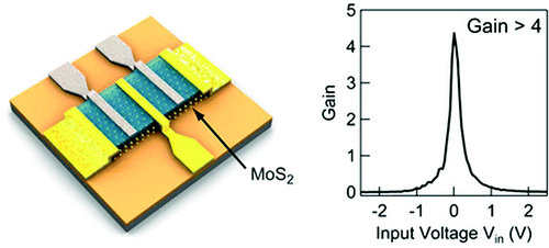
Molybdenite is on a par with silicon in terms of its ability to amplify electronic signals, with an output signal that is four times stronger than the incoming signal. This proves that there is “considerable potential for creating more complex chips,” Kis says. “With graphene, for example, this amplitude is about 1. Below this threshold, the output voltage would not be sufficient to feed a second, similar chip.”Built in flexibility
Molybdenite also has mechanical properties that make it interesting as a possible material for use in flexible electronics, such as eventually in the design of flexible sheets of chips. These could, for example, be used to manufacture computers that could be rolled up or devices that could be affixed to the skin.
Logic circuits and the ability to amplify electrical signals form the functional backbone of electronics along with the possibility to integrate multiple elements on the same chip. The miniaturization of electronic circuits is expected to reach fundamental limits in the near future. Two-dimensional materials such as single-layer MoS2 represent the ultimate limit of miniaturization in the vertical dimension, are interesting as building blocks of low-power nanoelectronic devices, and are suitable for integration due to their planar geometry. Because they are less than 1 nm thin, 2D materials in transistors could also lead to reduced short channel effects and result in fabrication of smaller and more power-efficient transistors. Here, we report on the first integrated circuit based on a two-dimensional semiconductor MoS2. Our integrated circuits are capable of operating as inverters, converting logical “1” into logical “0”, with room-temperature voltage gain higher than 1, making them suitable for incorporation into digital circuits. We also show that electrical circuits composed of single-layer MoS2 transistors are capable of performing the NOR logic operation, the basis from which all logical operations and full digital functionality can be deduced.
7 pages of supplemental information
Nextbigfuture had previously covered the potential of Molybdenite for computer chips
Molybdenite can make smaller and 100,000 times more energy-efficient electronic chips.
If you liked this article, please give it a quick review on ycombinator or StumbleUpon. Thanks

Brian Wang is a Futurist Thought Leader and a popular Science blogger with 1 million readers per month. His blog Nextbigfuture.com is ranked #1 Science News Blog. It covers many disruptive technology and trends including Space, Robotics, Artificial Intelligence, Medicine, Anti-aging Biotechnology, and Nanotechnology.
Known for identifying cutting edge technologies, he is currently a Co-Founder of a startup and fundraiser for high potential early-stage companies. He is the Head of Research for Allocations for deep technology investments and an Angel Investor at Space Angels.
A frequent speaker at corporations, he has been a TEDx speaker, a Singularity University speaker and guest at numerous interviews for radio and podcasts. He is open to public speaking and advising engagements.