

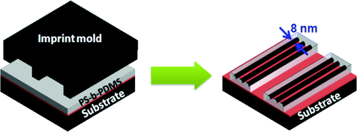
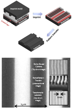
Directed self-assembly (DSA) of block copolymers (BCPs), either by selective wetting of surface chemical prepatterns or by graphoepitaxial alignment with surface topography, has ushered in a new era for high-resolution nanopatterning. These pioneering approaches, while effective, require expensive and time-consuming lithographic patterning of each substrate to direct the assembly. To overcome this shortcoming, nanoimprint molds—attainable via low-cost optical lithography—were investigated for their potential to be reusable and efficiently template the assembly of block copolymers (BCPs) while under complete confinement. Nanoimprint directed self-assembly conveniently avoids repetitive and expensive chemical or topographical prepatterning of substrates. To demonstrate this technique for high-resolution nanofabrication, we aligned sub-10 nm resolution nanopatterns using a cylinder-forming, organic–inorganic hybrid block copolymer, polystyrene-block-polydimethylsiloxane (PS-b-PDMS). Nanopatterns derived from oxidized PDMS microdomains were successfully transferred into the underlying substrate using plasma etching. In the development phase of this procedure, we investigated the role of mold treatments and pattern geometries as DSA of BCPs are driven by interfacial chemistry and physics. In the optimized route, silicon molds treated with PDMS surface brushes promoted rapid BCP alignment and reliable mold release while appropriate mold geometries provided a single layer of cylinders and negligible residual layers as required for pattern transfer. Molds thus produced were reusable to the same efficacy between nanoimprints. We also demonstrated that shear flow during the nanoimprint process enhanced the alignment of the BCP near open edges, which may be engineered in future schemes to control the BCP microdomain alignment kinetics during DSA.
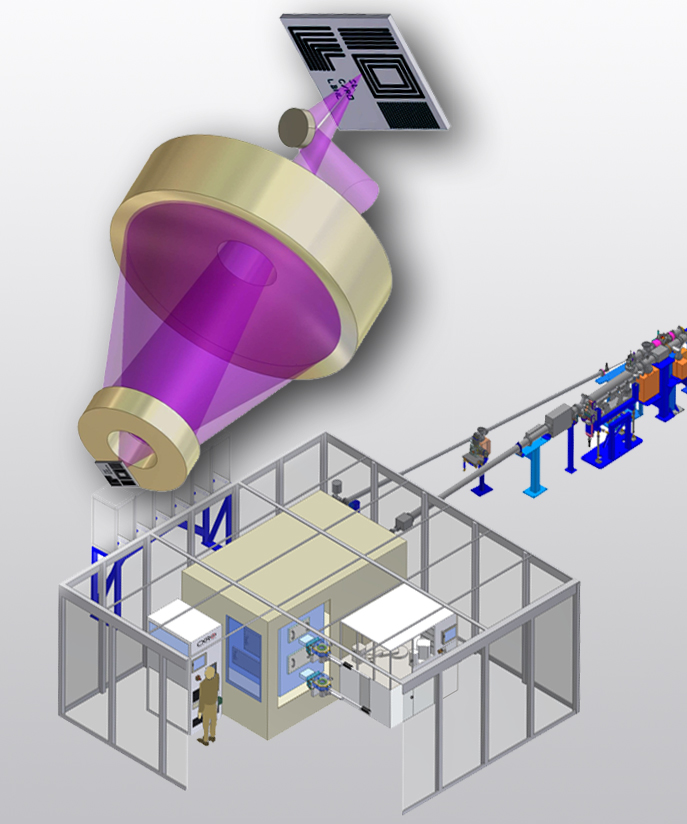
Berkeley National Laboratory (Berkeley Lab) to build facilities and instruments for advanced extreme-ultraviolet lithography (EUVL)
The MET5 microlithography tool at the Advanced Light Source’s beamline 12.0.1 will be housed in an enclosure inside a new clean room with wafer-processing facilities immediately adjacent, built by Berkeley Lab. The MET5 tool, funded by industry, incorporates a state-of-the-art, 8-nanometer optic.
20 nanometer soldering iron at the Berkeley Molecular Foundry
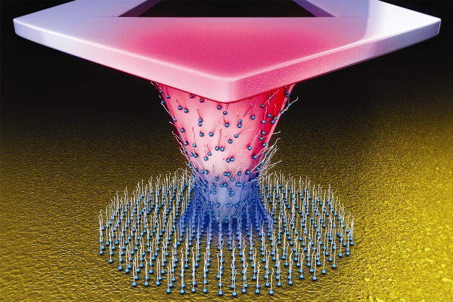
The collaborators developed a silicon-based AFM tip with a gradient of charge-carrying atoms sprinkled into the silicon such that a higher number reside at the base while fewer sit at the tip. This makes the tip heat up when electricity flows through it, much like the burner on an electric stove.
This ‘nanoheater’ can then be used to heat up inks applied to the tip, causing them to flow to the surface for fabricating microscale and nanoscale features. The group demonstrated this by drawing dots and lines of the organic molecule mercaptohexadecanoic acid on gold surfaces. The hotter the tip, the larger the feature size the team could draw.
“We are excited about this collaboration with Berkeley Lab, which combines their remarkable nanoscience capabilities with our technology to control temperature and heat flow on the nanometer scale,” says co-author William P. King, a University of Illinois professor of mechanical sciences and engineering. “Our ability to control the temperature within a nanometer-scale spot enabled this study of molecular-scale transport. By tuning the hotspot temperature, we can probe how molecules flow to a surface.”
“This thermal control over tip-to-surface transfer developed by Professor King’s group adds versatility by enabling on-the-fly variations in feature size and patterning of both liquid and solid materials,” DeYoreo adds.
If you liked this article, please give it a quick review on ycombinator or StumbleUpon. Thanks

Brian Wang is a Futurist Thought Leader and a popular Science blogger with 1 million readers per month. His blog Nextbigfuture.com is ranked #1 Science News Blog. It covers many disruptive technology and trends including Space, Robotics, Artificial Intelligence, Medicine, Anti-aging Biotechnology, and Nanotechnology.
Known for identifying cutting edge technologies, he is currently a Co-Founder of a startup and fundraiser for high potential early-stage companies. He is the Head of Research for Allocations for deep technology investments and an Angel Investor at Space Angels.
A frequent speaker at corporations, he has been a TEDx speaker, a Singularity University speaker and guest at numerous interviews for radio and podcasts. He is open to public speaking and advising engagements.