

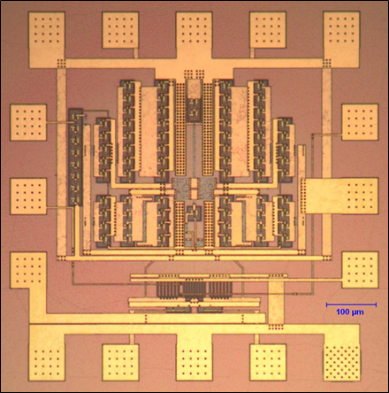
1. Chip-scale atomic clocks (CSAC) were first developed by DARPA and the National Institute of Standards and Technology (NIST) in 2004. These devices are smaller than traditional atomic clocks by a factor of 100 (down to about the size of a computer chip) and are more power-efficient by a factor of 10. Although CSACs are now commercially available, they have not yet been applied to space technologies.
On October 27, 2011, Progress 40 launched from Baikonur Cosmodrome carrying two DARPA CSACs, the first ever into space. The CSACs will soon be tested on board the International Space Station (ISS) in support of DARPA’s Micro-PNT (micro satellite positioning, navigation and timing) program. The chips will be inserted into bowling-ball sized satellites on the ISS called Synchronized Position, Hold, Engage and Reorient Experimental Satellites (SPHERES). Once the chips have been validated as operational, the SPHERES will perform a synchronized maneuver through the ISS cabin. After the experiment, the chips containing the CSACs will be removed and tested against the atomic clock onboard the ISS.
According to Thomas Lee, office director, DARPA Microsystems Technology Office, “Enabling the ability to ‘mix and match’ a wide variety of devices and materials on a common silicon substrate would allow circuit designers to select the best device for each function within their designs. This integration would provide DoD systems with the benefits of a variety of devices and materials integrated in close proximity on a single chip, minimizing the performance limitations caused by physical separation among devices.”
This effort also seeks to enable complex signal-processing and self-correction architectures to be brought to bear. The DAHI Foundry Technology effort hopes to establish a foundry capability for the production of chips using a wide range of heterogeneously integrated devices.
“DARPA anticipates bringing the compound semiconductor and silicon integrated circuit (IC) communities together for new ways to integrate components onto a single silicon wafer,” explained Sanjay Raman, DARPA program manager. “Such convergence would enable foundry-style production of high-performance microsystems, leveraging today’s silicon IC manufacturing base.”
If you liked this article, please give it a quick review on ycombinator or StumbleUpon. Thanks

Brian Wang is a Futurist Thought Leader and a popular Science blogger with 1 million readers per month. His blog Nextbigfuture.com is ranked #1 Science News Blog. It covers many disruptive technology and trends including Space, Robotics, Artificial Intelligence, Medicine, Anti-aging Biotechnology, and Nanotechnology.
Known for identifying cutting edge technologies, he is currently a Co-Founder of a startup and fundraiser for high potential early-stage companies. He is the Head of Research for Allocations for deep technology investments and an Angel Investor at Space Angels.
A frequent speaker at corporations, he has been a TEDx speaker, a Singularity University speaker and guest at numerous interviews for radio and podcasts. He is open to public speaking and advising engagements.