
Now we have shown that there is a way to achieve this transition without melting the material,” said Ritesh Agarwal, associate professor in the Department of Materials Science and Engineering in University of Pennsylvania’s School of Engineering and Applied Science, who conducted the research, along with members of his research group.. “We show that short electrical pulses of a few hundred nanosecond duration gradually induce disorder in the material until it amorphizes.”
Their advance was made possible by fashioning a PCM into thin nanowires, rather than a more bulky counterpart. This enabled the researchers to observe the phase change as it happened using a high-resolution transmission electron microscope at an atomic level of detail. Earlier researchers could only look at cross sections of their bulkier PCMs after the switching process was over.
Some kinds of memory, like a computer’s RAM, can switch between states very quickly, allowing for the computation necessary to run programs. But this kind of memory is “volatile” in that it needs a constant supply of power to maintain its states. Other kinds of memory, like the kind found on a flash drive, is non-volatile in that it retains its data even after the power is turned off. This kind of memory, however, has low switching speeds. Researchers have long attempted to find a “universal memory” which combines both non-volatility and high switching speeds, along with scalability, the ability to store large amounts of data.

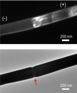
The top figure shows the jammed dislocation cloud, while the bottom shows the amorphous mark spanning the nanowire cross-section
Abstract – Phase-change materials undergo rapid and reversible crystalline-to-amorphous structural transformation and are being used for nonvolatile memory devices. However, the transformation mechanism remains poorly understood. We have studied the effect of electrical pulses on the crystalline-to-amorphous phase change in a single-crystalline Ge2Sb2Te5 (GST) nanowire memory device by in situ transmission electron microscopy. We show that electrical pulses produce dislocations in crystalline GST, which become mobile and glide in the direction of hole-carrier motion. The continuous increase in the density of dislocations moving unidirectionally in the material leads to dislocation jamming, which eventually induces the crystalline-to-amorphous phase change with a sharp interface spanning the entire nanowire cross section. The dislocation-templated amorphization explains the large on/off resistance ratio of the device.
Using nanowires enabled the researchers to observe the phase change as it happened using a high-resolution transmission electron microscope. Earlier researchers could only look at cross sections of their bulkier PCMs after the switching process was over.
By looking at the change in “real time,” the Penn researchers could see what effect the electrical pulses were having at an atomic level of detail.
“The pulses create ‘dislocations,’ which are planes of atoms removed from the crystal pattern, disrupting the order locally on an atomic length scale,” said Pavan Nukala, a co-author and member of the Agarwal group. “As we apply more and more pulses, the number of these dislocations start to increase.”
“Eventually, the dislocations start to move down the nanowire in the direction of the current,” Agarwal said. “At certain point, the number and density of dislocations becomes so huge that they jam in one spot.”
Like a traffic jam on a highway, the dislocations continue to pile up at that spot as more and more move down the length of the nanowire. At a critical point, the increasing disorder causes the material to amorphize the wire at the location of the jam.
The amorphous region, which always forms at the point of the jam and cuts through the entire cross section of the nanowire, is proof that this dislocation-based mechanism is fundamentally different from the melt-quench mechanism. With melting, the amorphous part should have spread along the surface of the material, rather than cut through its cross section.
“Having the surface amorphize doesn’t give us high resistance ratios because current can still travel through the crystalline interior,” Agarwal said. “Cutting across the entire nanowire completely blocks the current, making for a much better memory devices.
“With surface melting, you can increase the resistance a few times at most, but our observation that the resistance increased by two or three orders of magnitude is another evidence of the new mechanism.”
The PCM that researchers used in their study contained long tellurium-telluriumbonds that can easily slide apart, facilitating the planar dislocations that cause the material to amorphize.
The material, along with a better understanding of the mechanics of its phase change, will provide a starting point for picking the right qualities for future PCMs.
“If people think that melting is the only mechanism for phase change, then all the emphasis will be on making materials with low melting temperatures,” Agarwal said. “But we’ve shown that we need to do something else, which is to also look for materials that can create dislocations easily.”
22 pages of supplemental material has interesting pictures of the experimental setup and results
If you liked this article, please give it a quick review on ycombinator or StumbleUpon. Thanks

Brian Wang is a Futurist Thought Leader and a popular Science blogger with 1 million readers per month. His blog Nextbigfuture.com is ranked #1 Science News Blog. It covers many disruptive technology and trends including Space, Robotics, Artificial Intelligence, Medicine, Anti-aging Biotechnology, and Nanotechnology.
Known for identifying cutting edge technologies, he is currently a Co-Founder of a startup and fundraiser for high potential early-stage companies. He is the Head of Research for Allocations for deep technology investments and an Angel Investor at Space Angels.
A frequent speaker at corporations, he has been a TEDx speaker, a Singularity University speaker and guest at numerous interviews for radio and podcasts. He is open to public speaking and advising engagements.