Highly purified silicon represents up to 40 percent of the overall costs of conventional solar-cell arrays — so researchers have long sought to maximize power output while minimizing silicon usage. Now, a team at MIT has found a new approach that could reduce the thickness of the silicon used by more than 90 percent while still maintaining high efficiency.
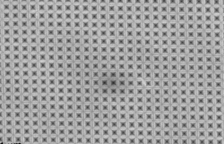
The secret lies in a pattern of tiny inverted pyramids etched into the surface of the silicon. These tiny indentations, each less than a millionth of a meter across, can trap rays of light as effectively as conventional solid silicon surfaces that are 30 times thicker.
The new findings are being reported in the journal Nano Letters in a paper by MIT postdoc Anastassios Mavrokefalos, professor Gang Chen, and three other postdocs and graduate students, all of MIT’s Department of Mechanical Engineering.
Seen from above, a sheet of silicon has been textured with an array of tiny inverted-pyramid shapes, so small that they correspond to the wavelengths of light and can efficiently trap light waves. Image: Anastassios Mavrokefalos
We see our method as enhancing the performance of thin-film solar cells,” Mavrokefalos says, but it would actually work for any silicon cells. “It would enhance the efficiency, no matter what the thickness,” he says.
Graduate student Matthew Branham, a co-author of the paper, says, “If you can dramatically cut the amount of silicon [in a solar cell] … you can potentially make a big difference in the cost of production. The problem is, when you make it very thin, it doesn’t absorb light as well.”
The operation of a solar cell occurs in two basic steps: First, an incoming particle of light, called a photon, enters and is absorbed by the material, rather than reflecting off its surface or passing right through. Second, electrons knocked loose from their atoms when that photon is absorbed then need to make their way to a wire where they can be harnessed to produce an electrical current, rather than just being trapped by other atoms.
Unfortunately, most efforts to increase the ability of thin crystalline silicon to trap photons — such as by creating a forest of tiny silicon nanowires on the surface — also greatly increase the material’s surface area, increasing the chance that electrons will recombine on the surface before they can be harnessed.
The new approach avoids that problem. The tiny surface indentations — the team calls them “inverted nanopyramids” — greatly increase light absorption, but with only a 70 percent increase in surface area, limiting surface recombination. Using this method, a sheet of crystalline silicon just 10 micrometers (millionths of a meter) thick can absorb light as efficiently as a conventional silicon wafer 30 times as thick.
That could not only reduce the amount of expensive, highly purified silicon needed to make the solar cells, Mavrokefalos explains, but also cut the weight of the cells, which in turn would reduce the material needed for frames and supports. The potential cost savings are “not only in the cell material, but also in the installation costs,” he says.
In addition, the technique developed by Mavrokefalos and his colleagues uses equipment and materials that are already standard parts of silicon-chip processing, so no new manufacturing machinery or chemicals would be required. “It’s very easy to fabricate,” Mavrokefalos says, yet “it attacks big problems.”
To create the tiny dents, the researchers use two sets of overlapping laser beams to produce exceptionally tiny holes in a layer of material — called a photoresist — that is deposited on top of the silicon. This interference lithography technique is scalable to a large area. Following several intermediate steps, a chemical called potassium hydroxide is used to dissolve away parts of the surface that were not covered by the photoresist. The crystal structure of silicon leads this etching process to produce the desired pyramidal shapes in the surface, Mavrokefalos says.
So far, the team has only carried out the first step toward making the new type of solar cells, producing the patterned surface on a silicon wafer and demonstrating its improvement in trapping light. The next step will be to add components to produce an actual photovoltaic cell and then show that its efficiency is comparable to that of conventional solar cells. The expectation is that the new approach should produce energy-conversion efficiencies of about 20 percent — compared to 24 percent for the best current commercial silicon solar cells — but this remains to be proved in practice.
If you liked this article, please give it a quick review on ycombinator or StumbleUpon. Thanks

Brian Wang is a Futurist Thought Leader and a popular Science blogger with 1 million readers per month. His blog Nextbigfuture.com is ranked #1 Science News Blog. It covers many disruptive technology and trends including Space, Robotics, Artificial Intelligence, Medicine, Anti-aging Biotechnology, and Nanotechnology.
Known for identifying cutting edge technologies, he is currently a Co-Founder of a startup and fundraiser for high potential early-stage companies. He is the Head of Research for Allocations for deep technology investments and an Angel Investor at Space Angels.
A frequent speaker at corporations, he has been a TEDx speaker, a Singularity University speaker and guest at numerous interviews for radio and podcasts. He is open to public speaking and advising engagements.


