

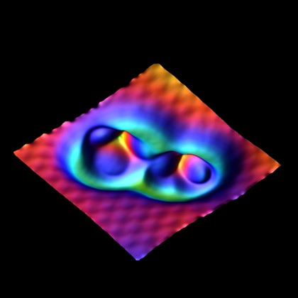
Atomic force microscopy (AFM) is used widely to study surfaces with a resolution on the nanometer scale – vastly inferior to atomic resolution offered by scanning tunneling microscopy (STM). In 1982, about a year after the invention of STM, the enigmatic Si 7×7 surface was resolved, a success that many view as the start of nanotechnology. In 1986, the AFM was introduced and hopes were high that resolving atoms in real space would soon be possible for insulators as well. However, profound problems appeared that originate in the physics of the tip-sample interaction and in the difficulties of measuring small forces. Today, the AFM exceeds the STM in spatial resolution, as shown in the image above that depicts a Fe dimer and a nearby Fe trimer adsorbed on a Cu(111) surface. A talk by Franz J. Giessibl, University of Regensburg, Germany talk discussed the steps in increasing resolution that also involved in changing the core of the AFM from a Si cantilever to a stiff, self-sensing piezoelectric cantilever (“qPlus sensor”). This sensor allows an uncompromised combination of STM/AFM, demonstrating atomic and subatomic spatial resolution in vacuum, low temperatures as well as in ambient conditions.
SOURCE – NIST

Brian Wang is a Futurist Thought Leader and a popular Science blogger with 1 million readers per month. His blog Nextbigfuture.com is ranked #1 Science News Blog. It covers many disruptive technology and trends including Space, Robotics, Artificial Intelligence, Medicine, Anti-aging Biotechnology, and Nanotechnology.
Known for identifying cutting edge technologies, he is currently a Co-Founder of a startup and fundraiser for high potential early-stage companies. He is the Head of Research for Allocations for deep technology investments and an Angel Investor at Space Angels.
A frequent speaker at corporations, he has been a TEDx speaker, a Singularity University speaker and guest at numerous interviews for radio and podcasts. He is open to public speaking and advising engagements.