

Foreseeable applications include integrating lasers, sensors, wave guides and other optical components into so-called lab-on-a-chip devices now used for disease diagnosis, screening experimental materials and drugs, DNA forensics and more. Easy to control, the new gold-catalyzed process for creating patterns of channels with nanoscale dimensions could help to spawn entirely new technologies fashioned from ensembles of ultra-small structures.
Preliminary research results that began as lemons—a contaminant-caused failure that impeded the expected formation of nanowires—eventually turned into lemonade when scanning electron microscope images revealed long, straight channels.
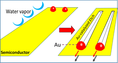
“We were disappointed, at first,” says NIST research chemist Babak Nikoobakht. “Then we figured out that water was the contaminant in the process—a problem that turned out to be a good thing.”
That’s because, as determined in subsequent experiments, the addition of water vapor served to transform gold nanoparticles into channel diggers, rather than the expected wire makers. Beginning with studies on the semiconductor indium phosphide, the team teased out the chemical mechanisms and necessary conditions underpinning the surface-etching process.

Electron micrograph of surface-directed nanochannels formed on the surface of the semiconductor indium phosphide. Nanochannels are formed using a gold-catalyzed vapor-liquid-solid etch process and their locations are defined by the deposited gold pattern. Credit: Marti/JILA

NANOLetters – Vapor–Liquid–Solid Etch of Semiconductor Surface Channels by Running Gold Nanodroplets
First, they patterned the surface of the semiconductor by selectively coating it with a gold layer only a few nanometers thick. Upon heating, the film breaks up into tiny particles that become droplets. The underlying indium phosphide dissolves into the gold nanoparticles above, creating a gold alloy. Then, heated water vapor is introduced into the system. At temperatures below 300 degrees Celsius (572 degrees Fahrenheit), the tiny gold-alloy particles, now swathed with water molecules, etch nanoscale pits into the indium phosphide.
But at 440 degrees Celsius (824 degrees Fahrenheit) and above, long V-shaped nanochannels formed. The channels followed straight paths dictated by the regularly repeating lattice of atoms in the crystalline semiconductor. During the process, indium and phosphorous atoms interact with oxygen atoms in the water molecules on the surface of the gold alloy droplet. The oxidized indium and phosphorous evaporate, and the droplet advances, picking up more semiconductor atoms to oxidize as it goes.
The result is a series of crystalline groves. The dimensions of the grooves correspond to the size of droplet, which can be controlled.
In effect, the droplet is the chemical equivalent of the auger on a snow blower that, instead of snow, burrows through the top portion of the semiconductor and ejects evaporated bits, Nikoobakht explains.
The team observed the same phenomena in gallium phosphide and indium arsenide, two more examples of semiconductors formed by combining elements from the third and fifth columns of the periodic table. Compound semiconductors in this class are used to make LEDs, and for communications, high-speed electronics and many other applications. Nikoobakht believes that, with adjustments, the etching process might also work for creating patterns of channels on silicon and other materials.
Controllable, fast and flexible, the “bottom up” channel-fabrication process shows promise for use on industrial scales, the researchers suggest. In their article, the teams describe how they used the process to etch patterns of hollow channels like those used to direct the flow of liquids, such as a blood sample, in a microfluidic device, or lab on a chip.
Abstract

Brian Wang is a Futurist Thought Leader and a popular Science blogger with 1 million readers per month. His blog Nextbigfuture.com is ranked #1 Science News Blog. It covers many disruptive technology and trends including Space, Robotics, Artificial Intelligence, Medicine, Anti-aging Biotechnology, and Nanotechnology.
Known for identifying cutting edge technologies, he is currently a Co-Founder of a startup and fundraiser for high potential early-stage companies. He is the Head of Research for Allocations for deep technology investments and an Angel Investor at Space Angels.
A frequent speaker at corporations, he has been a TEDx speaker, a Singularity University speaker and guest at numerous interviews for radio and podcasts. He is open to public speaking and advising engagements.