Taiwan Semiconductor Manufacturing Co. (TSMC), the world’s largest foundry, said it will fully implement extreme ultraviolet (EUV) lithography to make 5 nanometer chips by the end of this decade.
“We estimate that EUV will be a cost-effective tool for high-volume manufacturing by 2020, in time for our 5nm ramp,” TSMC Co-CEO Mark Liu said at an event to announce the company’s second-quarter results. “We plan to use EUV lithography extensively in 5nm to improve density, simplify process complexity and reduce cost.”
The company said it has been using 7nm as a development vehicle for EUV, achieving what it called good integration of EUV scanners, masks and photoresist. TSMC said it is running four state-of-the-art EUV scanners for infrastructure development and will move in another two NXE:3400 EUV production tools from ASML in the first quarter of 2017.
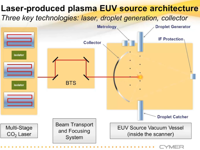
TSMC said it has implemented a 125 watt EUV source in its ASML NXE:3350 equipment to improve productivity. In the meantime, the company has also developed in-house EUV mask, material, inspection and repair technology to integrate its EUV lithography.
Up to now, the commercial viability of EUV has been in question. TSMC competitors such as Samsung appear more convinced about the commercial viability of EUV. A press report in South Korea said that Samsung plans to use EUV at 7 nanometers.
TSMC said it will see its first revenue from 10nm during the first quarter of 2017, and it expects 10nm to ramp steeply throughout next year.
“Our 10nm has been transferred from R&D to production,” Liu said. “Our first 10nm customer product has been produced with satisfactory functional yield. So far, three customer products have been taped out to us.”
At the 7nm node, TSMC said its yield improvement on a 256 megabit SRAM test device is ahead of schedule.
“We believe our 7nm power, performance and area density (PPA) is ahead of our competitors,” Liu said. TSMC’s mobile and high-performance computing customers “all have aggressive product tape out plans in the first half of 2017 with volume production planned in early 2018,” he added.
Boosting Capital Expenditure TSMC said it will raise its capital expenditure target for 2016 from an earlier range of $9 billion-$10 billion to a new range of $9.5 billion to $10.5 billion because expectations for 2017 mobile revenue have improved.
The company is expected to have the second-largest capex in the semiconductor industry this year, following Samsung. While analysts are saying the overall semiconductor industry may be headed for a slump this year, TSMC is maintaining a more sanguine outlook.
EUV Is Required for 7 nm Technology, But Will Be Implemented “When It’s Done”
In general, the industry remains rather optimistic about EUV lithography thanks to two years of solid progress. All leading makers of semiconductors, including Intel, TSMC, Samsung and GlobalFoundries plan to use EUV tools as soon as it makes sense. All four chipmakers indicated on various occasions in the recent months that EUV lithography will be required for 7 nm manufacturing technology. At the SPIE conference, TSMC and Samsung re-affirmed plans to insert EUVL into 7 nm production. By contrast, Intel indicated that while it would prefer to use EUVL for critical layers at 7 nm, it would only use the tech when it is completely ready. At present, Intel is experimenting with EUV on its 14 nm pilot fab line and the results have been encouraging, according to the company. Nonetheless, Intel believes that to make EUV a reality, in addition to many other things, the industry needs to improve yields, decrease costs and develop an ecosystem of EUV photomasks.
SOURCES- TSMC, Samsung, EEtimes, Cymer, Intel, Anandtech

Brian Wang is a Futurist Thought Leader and a popular Science blogger with 1 million readers per month. His blog Nextbigfuture.com is ranked #1 Science News Blog. It covers many disruptive technology and trends including Space, Robotics, Artificial Intelligence, Medicine, Anti-aging Biotechnology, and Nanotechnology.
Known for identifying cutting edge technologies, he is currently a Co-Founder of a startup and fundraiser for high potential early-stage companies. He is the Head of Research for Allocations for deep technology investments and an Angel Investor at Space Angels.
A frequent speaker at corporations, he has been a TEDx speaker, a Singularity University speaker and guest at numerous interviews for radio and podcasts. He is open to public speaking and advising engagements.


