

The Rice lab of theoretical physicist Boris Yakobson analyzed hybrids that put 2-D materials like graphene and boron nitride side by side to see what happens at the border. They found that the electronic characteristics of such “co-planar” hybrids differ from bulkier components.
Their results appear this month in the American Chemical Society journal Nano Letters.
Shrinking electronics means shrinking their components. Academic labs and industries are studying how materials like graphene may enable the ultimate in thin devices by building all the necessary circuits into an atom-thick layer.
“Our work is important because semiconductor junctions are a big field,” Yakobson said. “There are books with iconic models of electronic behavior that are extremely well-developed and have become the established pillars of industry.
“But these are all for bulk-to-bulk interfaces between three-dimensional metals,” he said. “Now that people are actively working to make two-dimensional devices, especially with co-planar electronics, we realized that the rules have to be reconsidered. Many of the established models utilized in industry just don’t apply.”
The researchers led by Rice graduate student Henry Yu built computer simulations that analyze charge transfer between atom-thick materials.
“It was a logical step to test our theory on both metals and semiconductors, which have very different electronic properties,” Yu said. “This makes graphene, which is a metal — or a semimetal, to be precise — molybdenum disulfide and boron nitride, which are semiconductors, or even their hybrids ideal systems to study.
“In fact, these materials have been widely fabricated and used in the community for almost a decade, which makes analysis of them more appreciable in the field. Furthermore, both hybrids of graphene-molybdenum disulfide and graphene-boron nitride have been successfully synthesized recently, which means our study has practical meaning and can be tested in the lab now,” he said.
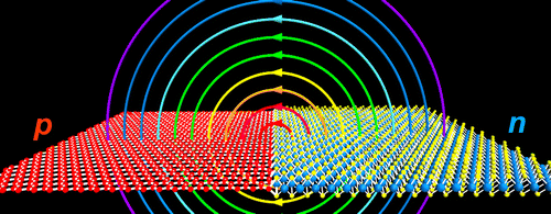
Yakobson said 3-D materials have a narrow region for charge transfer at the positive and negative (or p/n) junction. But the researchers found that 2-D interfaces created “a highly nonlocalized charge transfer” — and an electric field along with it — that greatly increased the junction size. That could give them an advantage in photovoltaic applications like solar cells, the researchers said.
The lab built a simulation of a hybrid of graphene and molybdenum disulfide and also considered graphene-boron nitride and graphene in which half was doped to create a p/n junction. Their calculations predicted the presence of an electric field should make 2-D Schottky (one-way) devices like transistors and diodes more tunable based on the size of the device itself.
How the atoms line up with each other is also important, Yakobson said. Graphene and boron nitride both feature hexagonal lattices, so they mesh perfectly. But molybdenum disulfide, another promising material, isn’t exactly flat, though it’s still considered 2-D.
“If the atomic structures don’t match, you get dangling bonds or defects along the borderline,” he said. “The structure has consequences for electronic behavior, especially for what is called Fermi level pinning.”
Pinning can degrade electrical performance by creating an energy barrier at the interface, Yakobson explained. “But your Schottky barrier (in which current moves in only one direction) doesn’t change as expected. This is a well-known phenomenon for semiconductors; it’s just that in two dimensions, it’s different, and in this case may favor 2-D over 3-D systems.”
Yakobson said the principles put forth by the new paper will apply to patterned hybrids of two or more 2-D patches. “You can make something special, but the basic effects are always at the interfaces. If you want to have many transistors in the same plane, it’s fine, but you still have to consider effects at the junctions.
“There’s no reason we can’t build 2-D rectifiers, transistors or memory elements,” he said. “They’ll be the same as we use routinely in devices now. But unless we develop a proper fundamental knowledge of the physics, they may fail to do what we design or plan.”
Abstract
With the lateral coplanar heterojunctions of two-dimensional monolayer materials turning into reality, the quantitative understanding of their electronic, electrostatic, doping, and scaling properties becomes imperative. In contrast to traditional bulk 3D junctions where carrier equilibrium is reached through local charge redistribution, a highly nonlocalized charge transfer (trailing off as 1/x away from the interface) is present in lateral 2D junctions, increasing the junction size considerably. The depletion width scales as p–1, while the differential capacitance varies very little with the doping level p. The properties of lateral 2D junctions are further quantified through numerical analysis of realistic materials, with graphene, MoS2, and their hybrid serving as examples. Careful analysis of the built-in potential profile shows strong reduction of Fermi level pinning, suggesting better control of the barrier in 2D metal–semiconductor junctions.
SOURCES – Rice University, Nanoletters

Brian Wang is a Futurist Thought Leader and a popular Science blogger with 1 million readers per month. His blog Nextbigfuture.com is ranked #1 Science News Blog. It covers many disruptive technology and trends including Space, Robotics, Artificial Intelligence, Medicine, Anti-aging Biotechnology, and Nanotechnology.
Known for identifying cutting edge technologies, he is currently a Co-Founder of a startup and fundraiser for high potential early-stage companies. He is the Head of Research for Allocations for deep technology investments and an Angel Investor at Space Angels.
A frequent speaker at corporations, he has been a TEDx speaker, a Singularity University speaker and guest at numerous interviews for radio and podcasts. He is open to public speaking and advising engagements.