

DARPA and MIT are leading an effort to take what are now bulky expensive Light Imaging, Detection, And Ranging (LIDAR) systems and make them small enough to fit on a microchip.
LIDAR is one of the key parts of Google’s self driving car.
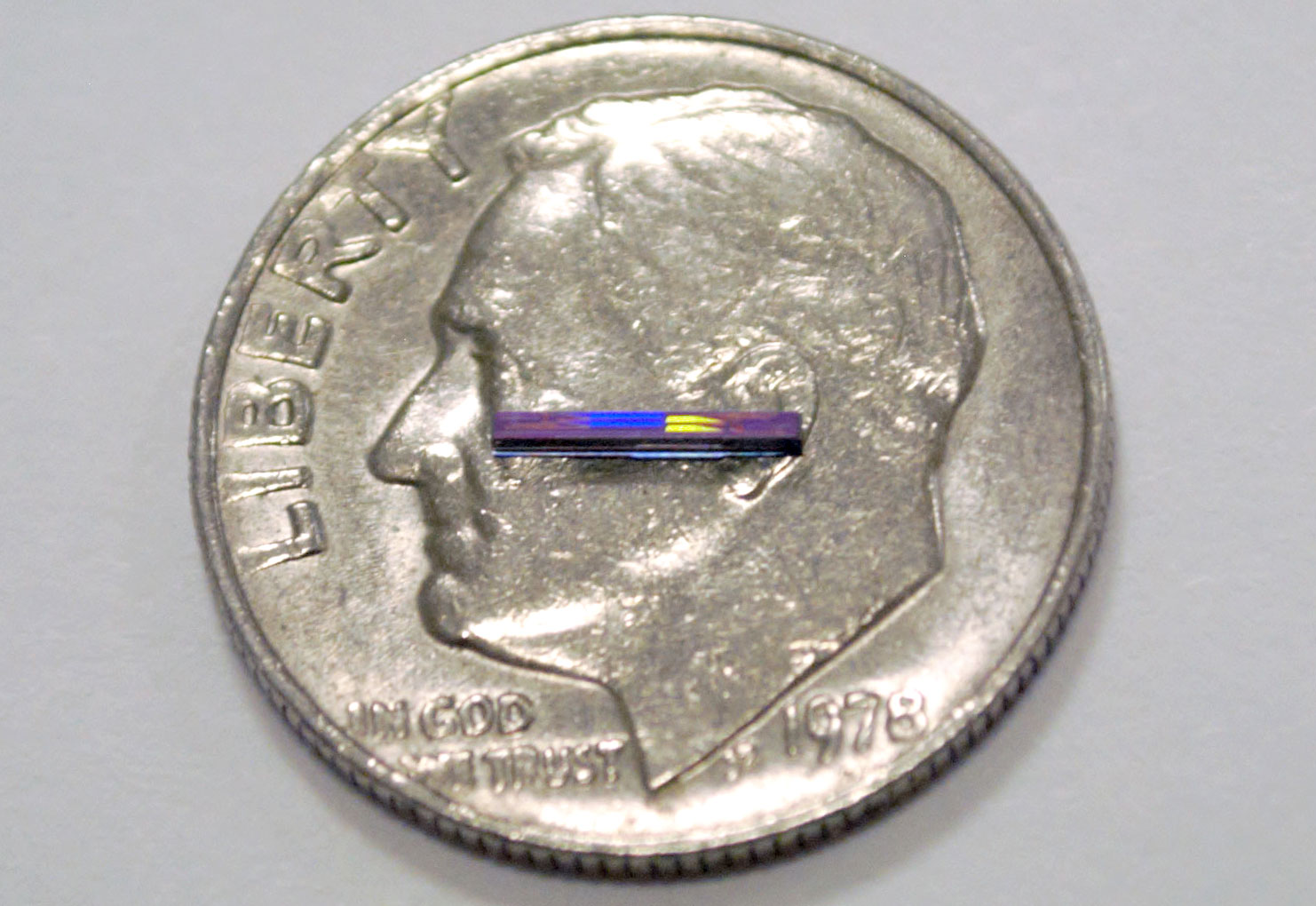
MIT’s Photonic Microsystems Group is developing a lidar-on-a-chip system that is smaller than a dime, has no moving parts, and could be mass-produced at a very low cost for use in self-driving cars, drones, and robots.
Light detection and ranging, or lidar, is a sensing technology based on laser light. It’s similar to radar, but can have a higher resolution, since the wavelength of light is about 100,000 times smaller than radio wavelengths. For robots, this is very important: Since radar cannot accurately image small features
By bringing down LIDAR’s size and costs the project could spark a technological revolution like that from the miniaturization of cameras for mobile phones, Josh Conway, programme manager of the Microsystems Technology Office for DARPA.
Today, commercially available high-end lidar systems can range from $1,000 to upwards of $70,000, which can limit their applications where cost must be minimized.
The new lidar chips are produced on 300-millimeter wafers, making their potential production cost on the order of $10 each at production volumes of millions of units per year. They also have the potential to be much more robust because of the lack of moving parts, with a non-mechanical beam steering 1,000 times faster than what is currently achieved in mechanical lidar systems.
The chip is enabled by development of 300-mm silicon photonics.
At the moment, our on-chip lidar system can detect objects at ranges of up to 2 meters, though we hope to achieve a 10-meter range within a year. The minimum range is around 5 centimeters. We have demonstrated centimeter longitudinal resolution and expect 3-cm lateral resolution at 2 meters. There is a clear development path towards lidar on a chip technology that can reach 100 meters, with the possibility of going even farther.
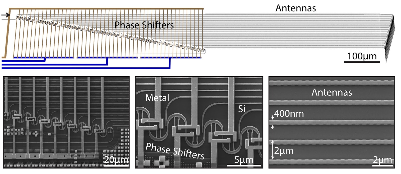
Using other materials in the chip (such as silicon nitride) will allow for an increase in power output of two to three orders of magnitude.
After long range LIDAR chip – 40 Gb/s communication chips and holography chip
DARPA has recently created a follow-up program called Modular Optical Aperture Building Blocks (MOABB), which is focused on extending this silicon photonic lidar work in the coming years. Though the MOABB program is not a part of our academic research group, after the lidar effort of the E-PHI program ends, we plan to extend our phased array work to free-space communications to allow for multiple photonic chips to interface with each other with over 40Gb/s data rates. We are also developing visible light phased arrays with applications such as Li-Fi and holography that can be seen by the human eye.
E-PHI seeks to develop the necessary technologies, architectures and design innovations to enable novel chip-scale electronic-photonic/mixed-signal integrated circuits on a common silicon substrate. It is envisioned that E-PHI technology will enable a wide range of novel chip-scale optoelectronic microsystems, including coherent optical systems for sensing (LADAR) and communications, optical arbitrary waveform generators and multi-wavelength imagers with integrated image processing and readout circuitry. To validate the feasibility and viability of electronic-photonic heterogeneous integration technology, E-PHI aims to demonstrate novel high-performance heterogeneous electronic-photonic integrated microsystems. It is anticipated that these E-PHI demonstrator microsystems will provide considerable performance improvement and size reduction versus current, state-of-the-art technologies.
SOURCES- IEEE Spectrum, MIT, DARPA, IHS Janes

Brian Wang is a Futurist Thought Leader and a popular Science blogger with 1 million readers per month. His blog Nextbigfuture.com is ranked #1 Science News Blog. It covers many disruptive technology and trends including Space, Robotics, Artificial Intelligence, Medicine, Anti-aging Biotechnology, and Nanotechnology.
Known for identifying cutting edge technologies, he is currently a Co-Founder of a startup and fundraiser for high potential early-stage companies. He is the Head of Research for Allocations for deep technology investments and an Angel Investor at Space Angels.
A frequent speaker at corporations, he has been a TEDx speaker, a Singularity University speaker and guest at numerous interviews for radio and podcasts. He is open to public speaking and advising engagements.