

The electronic data connections within and between microchips are increasingly becoming a bottleneck in the exponential growth of data traffic worldwide. Optical connections are the obvious successors but optical data transmission requires an adequate nanoscale light source, and this has been lacking. Scientists at Eindhoven University of Technology (TU/e) now have created a light source that has the right characteristics: a nano-LED that is 1000 times more efficient than its predecessors, and is capable of handling gigabits per second data speeds. They have published their findings in the online journal Nature Communications.
With electrical cables reaching their limits, optical connections like fiberglass are increasingly becoming the standard for data traffic. Over longer distances almost all data transmission is optical. Within computer systems and microchips, too, the growth of data traffic is exponential, but that traffic is still electronic, and this is increasingly becoming a bottleneck. Since these connections (‘interconnects’) account for the majority of the energy consumed by chips, many scientists around the world are working on enabling optical (photonic) interconnects. Crucial to this is the light source that converts the data into light signals which must be small enough to fit into the microscopic structures of microchips. At the same time, the output capacity and efficiency have to be good. Especially the efficiency is a challenge, as small light sources, powered by nano- or microwatts, have always performed very inefficiently to date.
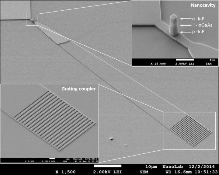
This is a scanning electron microscope picture of the new nano-LED, including some details. CREDIT Eindhoven University of Technology
Nature Communications – Waveguide-coupled nanopillar metal-cavity light-emitting diodes on silicon
Researchers at TU Eindhoven have now developed a light-emitting diode (LED) of some hundred nanometers with an integrated light channel (waveguide) to transport the light signal. This integrated nano-LED is a 1000 times more efficient than the best variants developed elsewhere. The Eindhoven-based researchers have especially made progress in the quality of the integrated coupling of the light source and the waveguide whereby much less light is lost and therefore far more light enters the waveguide. The efficiency of the new nano-LED currently lies between 0.01 and 1 percent, but the researchers expect to be well above that figure soon thanks to a new production method.
Another key characteristic of the new nano-LED is that it is integrated into a silicon substrate on a membrane of indium phosphide. Silicon is the basic material for microchips but is not suitable for light sources whereas indium phosphide is. Furthermore, tests reveal that the new element converts electrical signals rapidly into optical signals and can handle data speeds of several gigabits per second.
The researchers in Eindhoven believe that their nano-LED is a viable solution that will take the brake off the growth of data traffic on chips. However, they are cautious about the prospects. The development is not yet at the stage where it can be exploited by the industry and the production technology that is needed still has to get off the ground.
The development of high-density optical interconnects with reduced energy consumption has been identified as one of the major challenges in future computing and communication systems. A new generation of photonic devices, integrated within or on top of a complementary metal-oxide-semiconductor (CMOS) chip, is therefore needed, featuring unprecedented levels of integration density, speed and energy efficiency. For the light sources, the most promising performance on silicon has been achieved by ring lasers based on III–V active layers bonded on silicon. These hybrid III–V/Si devices have however a relatively large footprint (several tens of μm2) and present a power consumption far exceeding the requirements of future interconnects. On the ther hand, in the last decade, a new class of nanophotonic light sources has emerged which use either photonic crystals or metallic layers to achieve strong optical confinement, eventually leading to ultralow-threshold lasing and other interesting effects, such as spontaneous emission enhancement via the Purcell factor. While low-threshold photonic crystal lasers on InP have been demonstrated, their device footprint also remains relatively large (tens of μm2) and integration on silicon has been demonstrated only very recently
Researchers here presented a metal-cavity nanopillar LED on a silicon substrate working at telecommunications wavelengths (1.55 μm), coupled to an InP-membrane waveguide. With this approach we demonstrate full compatibility with the InP membranes on silicon (IMOS) integration platform25, in which a III–V photonic layer provides the optical functionality and the silicon substrate hosts electronics. The devices show nW (tens of nW) measured output powers at ∼100 μA (∼10 μA) current injection levels, at room and low temperature, respectively. When corrected for the outcoupling and setup collection efficiency, this corresponds to waveguide-coupled powers of 22 nW (300 K) and 336 nW (9.5 K) and an on-chip external quantum efficiency (EQE), ηQE, ranging from 10−4 (300 K) to 10−2 (9.5 K). Dynamic characterization via time-correlated single-photon counting measurements reveals sub-nanosecond electro-optical response and we confirm that such fast modulation is possible due to a strong non-radiative recombination. The reported data together with numerical simulations show the potential of metal-cavity nanopillar LEDs for efficient low-power interconnects operating at Gb/s data rates
In summary, we present a waveguide-coupled nanopillar LED device with metal-cavity, fabricated in a III–V layer stack bonded to a silicon substrate. The device shows relatively high on-chip external quantum efficiency (10−4 to 10−2 for room-temperature and 9.5 K, respectively) and output power (that is, nW to tens of nW) far exceeding previous nanoscale LEDs exhibiting up to hundreds of pW output
Abstract
Nanoscale light sources using metal cavities have been proposed to enable high integration density, efficient operation at low energy per bit and ultra-fast modulation, which would make them attractive for future low-power optical interconnects. For this application, such devices are required to be efficient, waveguide-coupled and integrated on a silicon substrate. We demonstrate a metal-cavity light-emitting diode coupled to a waveguide on silicon. The cavity consists of a metal-coated III–V semiconductor nanopillar which funnels a large fraction of spontaneous emission into the fundamental mode of an InP waveguide bonded to a silicon wafer showing full compatibility with membrane-on-Si photonic integration platforms. The device was characterized through a grating coupler and shows on-chip external quantum efficiency in the 10−4–10−2 range at tens of microamp current injection levels, which greatly exceeds the performance of any waveguide-coupled nanoscale light source integrated on silicon in this current range. Furthermore, direct modulation experiments reveal sub-nanosecond electro-optical response with the potential for multi gigabit per second modulation speeds.

Brian Wang is a Futurist Thought Leader and a popular Science blogger with 1 million readers per month. His blog Nextbigfuture.com is ranked #1 Science News Blog. It covers many disruptive technology and trends including Space, Robotics, Artificial Intelligence, Medicine, Anti-aging Biotechnology, and Nanotechnology.
Known for identifying cutting edge technologies, he is currently a Co-Founder of a startup and fundraiser for high potential early-stage companies. He is the Head of Research for Allocations for deep technology investments and an Angel Investor at Space Angels.
A frequent speaker at corporations, he has been a TEDx speaker, a Singularity University speaker and guest at numerous interviews for radio and podcasts. He is open to public speaking and advising engagements.