

Intel remains confident about scaling CMOS and extending Moore’s law beyond 2024
Someday we may reach a physical limit. But Intel does not see that point on their horizon.
1990, when the features on the wafer were the same size as the wavelength of the light we used to print them: 193 nm. Physics was very clear. We couldn’t go any further.
But we met that challenge. We printed with the interference fringes from the patterns on the masks. We developed computational lithography and multiple patterning. In retrospect, 193 nm wasn’t even a speed bump, and today we are doing 20 times better than that because of continued innovations like FinFET transistors and hyper scaling, which we implemented with our current 14 nm process. Today we’re talking more about further hyper scaling enhancements for our upcoming 10 nm process and how, thanks to this new process breakthrough, we continue to realize the same cost-per-million transistors.
How are we doing this? In historical Intel fashion we’ve continued to push through the barriers by identifying challenges, isolating them and solving them. Nearby, we see some specific challenges we must solve soon. That’s where we are today with 7 nm. Further out, we see challenges that might have several alternative solutions. We pursue them all until it is clear which will work best. We are always looking three generations – seven to nine years – ahead. Today we have line of sight to 7 and 5 nm. We may not know exactly which approaches will prove best for 5 nm yet, but our culture thrives on those challenges. It has for generations.
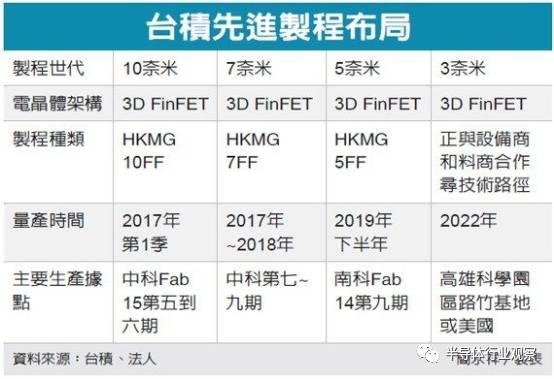
Taiwan Semiconductor Manufacturing Co. (TSMC) said that it plans to build its next fab for chips made at the 5-nm to 3-nm technology node as early as 2022 as it aims for industry leadership.

Brian Wang is a Futurist Thought Leader and a popular Science blogger with 1 million readers per month. His blog Nextbigfuture.com is ranked #1 Science News Blog. It covers many disruptive technology and trends including Space, Robotics, Artificial Intelligence, Medicine, Anti-aging Biotechnology, and Nanotechnology.
Known for identifying cutting edge technologies, he is currently a Co-Founder of a startup and fundraiser for high potential early-stage companies. He is the Head of Research for Allocations for deep technology investments and an Angel Investor at Space Angels.
A frequent speaker at corporations, he has been a TEDx speaker, a Singularity University speaker and guest at numerous interviews for radio and podcasts. He is open to public speaking and advising engagements.