
After four years of development, University of Sydney scientists say the Internet is set to become on average 60 times faster than existing networks.
“The scratched glass we’ve developed is actually a photonic integrated circuit,” Eggleton said.
“This circuit uses the ‘scratch’ as a guide or a switching path for information – like when trains are switched from one track to another – except this switch takes only one picosecond to change tracks. This means that in one second the switch is turning on and off about one million times. We are talking about photonic technology that has terabit per second capacity.”
An initial demonstration proved it possible to achieve speeds 60 times faster than existing local networks.
Ultrahigh nonlinear tapered fiber and planar rib Chalcogenide waveguides have been developed to enable high-speed all-optical signal processing in compact, low-loss optical devices through the use of four-wave mixing (FWM) and cross-phase modulation (XPM) via the ultra fast Kerr effect. Tapering a commercial $hbox{As}_{2}hbox{Se}_{3}$ fiber is shown to reduce its effective core area and enhance the Kerr nonlinearity thereby enabling XPM wavelength conversion of a 40 Gb/s signal in a shorter 16-cm length device that allows a broader wavelength tuning range due to its smaller net chromatic dispersion. Progress toward photonic chip-scale devices is shown by fabricating $hbox{As}_{2}hbox{S}_{3}$ planar rib waveguides exhibiting nonlinearity up to $2080, {rm W}^{-1}cdot hbox{km}^{-1}$ and losses as low as 0.05 dB/cm. The material’s high refractive index, ensuring more robust confinement of the optical mode, permits a more compact serpentine-shaped rib waveguide of 22.5 cm length on a 7-cm-size chip, which is successfully applied to broadband wavelength conversion of 40–80 Gb/s signals by XPM. A shorter 5-cm length planar waveguide proves most effective for all-optical time-division demultiplexing of a 160 Gb/s signal by FWM and analysis shows its length is near optimum for maximizing FWM in consideration of its dispersion and loss.
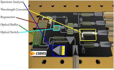
Speeding up the Internet 100 times is just a stepping stone to a Photonic Chip
The Centre for Ultrahigh bandwidth Devices for Optical Systems (CUDOS) vision is the Photonic Chip.


FURTHER READING
Centre for Ultrahigh bandwidth Devices for Optical Systems (CUDOS) Research
All-optical and nonlinear signal processing
Microstructured and tapered fibre devices
Optical waveguide gratings and slow light
So why use microfluidics in conjunction with microphotonics? The combination of these fields potentially allows one to impart adjustable photonic control in new ways that are highly compact and tuneable. We may also turn the technology around and use photonics to sense fluid properties, which is of increasing importance to medical diagnostics.

Brian Wang is a Futurist Thought Leader and a popular Science blogger with 1 million readers per month. His blog Nextbigfuture.com is ranked #1 Science News Blog. It covers many disruptive technology and trends including Space, Robotics, Artificial Intelligence, Medicine, Anti-aging Biotechnology, and Nanotechnology.
Known for identifying cutting edge technologies, he is currently a Co-Founder of a startup and fundraiser for high potential early-stage companies. He is the Head of Research for Allocations for deep technology investments and an Angel Investor at Space Angels.
A frequent speaker at corporations, he has been a TEDx speaker, a Singularity University speaker and guest at numerous interviews for radio and podcasts. He is open to public speaking and advising engagements.
Comments are closed.