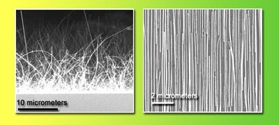
Randomly oriented nanowires, on the growth substrate at left, are having a “bad hair day.” But after contact printing, the nanowires on the receiver substrate are highly aligned.
The Javey group has devised two printing methods, contact and roller. The roller method involves growing nanowires on the surface of a cylinder and rolling it across the application substrate, like painting with a paint roller.
Contact printing involves growing nanowires on a flat substrate, inverting it, and pressing it onto the desired substrate. Then the nanowires are detached by sliding the growth substrate away, leaving them attached to the application substrate. Due to the lack of strong surface chemical interactions between nanowires, the process is self-limited to the transfer of only one layer of nanowires. The printed nanowires are highly aligned in the direction of the sliding.
For their integrated nanowire photosensor circuitry, the Javey group used cadmium selenide nanowires as visible-light sensors. For the electronics, nanowires with a germanium core and a silicon shell were the basis of field-effect transistors that would amplify the current produced by the photosensors in response to light by five orders of magnitude.
Results of the Javey group’s integrated nanowire circuit showed successful photoresponse in 80 percent of the circuits, with fairly small variations among them. Where circuits did fail, the causes were due to defects in fabrication of the circuit connections (10 percent), failure in photosensor printing (5 percent), or defective nanowires (5 percent). The relatively high yield of complex operational circuits proved the potential of the technology, with improvements readily achievable by optimizing nanowire synthesis and fabrication of the devices.

Artist’s impression of an integrated light sensor circuit based on nanowire arrays (Javey Group).

Brian Wang is a Futurist Thought Leader and a popular Science blogger with 1 million readers per month. His blog Nextbigfuture.com is ranked #1 Science News Blog. It covers many disruptive technology and trends including Space, Robotics, Artificial Intelligence, Medicine, Anti-aging Biotechnology, and Nanotechnology.
Known for identifying cutting edge technologies, he is currently a Co-Founder of a startup and fundraiser for high potential early-stage companies. He is the Head of Research for Allocations for deep technology investments and an Angel Investor at Space Angels.
A frequent speaker at corporations, he has been a TEDx speaker, a Singularity University speaker and guest at numerous interviews for radio and podcasts. He is open to public speaking and advising engagements.

