

Terahertz near field nanoscope has 40 nanometer resolution.
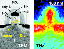
Nanoscale resolution is achieved by THz field confinement at the very tip apex to within 30 nm, which is in good agreement with full electro-dynamic calculations. Imaging semiconductor transistors, we provide first evidence of 40 nm (λ/3000) spatial resolution at 2.54 THz (wavelength λ = 118 μm) and demonstrate the simultaneous THz recognition of materials and mobile carriers in a single nanodevice. Fundamentally important, we find that the mobile carrier contrast can be directly related to near-field excitation of THz-plasmons in the doped semiconductor regions. This opens the door to quantitative studies of local carrier concentration and mobility at the nanometer scale. The THz near-field response is extraordinary sensitive, providing contrast from less than 100 mobile electrons in the probed volume. Future improvements could allow for THz characterization of even single electrons or biomolecules.
Nanowerk has some more information.
This was made possible by the use of extreme THz field concentration at the sharp tip of a scanning atomic force microscope (AFM). The THz nanoscope thus breaks the diffraction barrier by a factor of 1500, and with its 40 nm resolving power matches the needs of modern nanoscience and technology.
THz illumination offers a 100-fold increased sensitivity to the conductivity of semiconducting materials when compared to infrared light. This extreme sensitivity is difficult to achieve by any other optical microscopy technique, rendering the described microscopy technique highly desirable for quality assurance and analysis of failure mechanisms in industrially produced semiconductor nanodevices.

Brian Wang is a Futurist Thought Leader and a popular Science blogger with 1 million readers per month. His blog Nextbigfuture.com is ranked #1 Science News Blog. It covers many disruptive technology and trends including Space, Robotics, Artificial Intelligence, Medicine, Anti-aging Biotechnology, and Nanotechnology.
Known for identifying cutting edge technologies, he is currently a Co-Founder of a startup and fundraiser for high potential early-stage companies. He is the Head of Research for Allocations for deep technology investments and an Angel Investor at Space Angels.
A frequent speaker at corporations, he has been a TEDx speaker, a Singularity University speaker and guest at numerous interviews for radio and podcasts. He is open to public speaking and advising engagements.