

Fujitsu Laboratories developed novel technology that allows for graphene to be formed on insulating film substrate via CVD at the low fabrication-temperature of 650°C, enabling graphene-based transistors to be directly formed on the entire surface of substrates. Although the test substrate employed was a 75-mm silicon substrate (wafer) with oxide film, the new technique is applicable to larger 300-mm wafers as well.
1. Low-temperature synthesis of multi-layer graphene featuring thickness controlled via CVD, on entire surface of substrate
2. Process for forming transfer-free graphene transistors

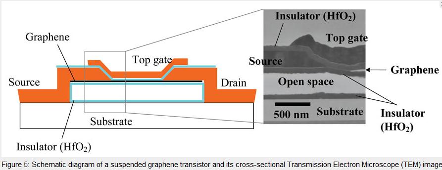
Fujitsu Laboratories also developed a process for forming transistors that use graphene as the channel material, as outlined in the picture. This process is independent of wafer size, so it can be applied to large-scale substrates.
1. First, an iron catalyst is formed into the desired channel shape, using a conventional photolithographic process.
2. Graphene is then formed on the iron layer via CVD.
3. Source and drain electrodes of titanium-gold film are formed at both ends of the graphene, thereby “fixing” the graphene.
4. Next, just the iron catalyst is removed using acid, leaving the graphene suspended between the source and drain electrodes, with the graphene “bridged” between the electrodes.
5. Using atomic-layer deposition (ALD), a method for forming thin films, a layer of hafnium dioxide (HfO2) is grown on top of the graphene to stabilize the graphene.
6. Finally, a gate electrode is formed on top of the graphene and through the HfO2, resulting in the formation of a graphene transistor.

Brian Wang is a Futurist Thought Leader and a popular Science blogger with 1 million readers per month. His blog Nextbigfuture.com is ranked #1 Science News Blog. It covers many disruptive technology and trends including Space, Robotics, Artificial Intelligence, Medicine, Anti-aging Biotechnology, and Nanotechnology.
Known for identifying cutting edge technologies, he is currently a Co-Founder of a startup and fundraiser for high potential early-stage companies. He is the Head of Research for Allocations for deep technology investments and an Angel Investor at Space Angels.
A frequent speaker at corporations, he has been a TEDx speaker, a Singularity University speaker and guest at numerous interviews for radio and podcasts. He is open to public speaking and advising engagements.