

Ultra-high-density data storage is now a step closer thanks to an advance in device fabrication achieved by Bao-Yu Zong and co-workers from the Data Storage Institute of A*STAR in Singapore. Devices for data-storage applications are created by depositing a ‘resist’ material onto a substrate, which is etched into a pattern using an electron beam and then used as a guide for depositing the device materials before being washed away. Zong and co-workers mixed metallic nanoparticles into commercially available resists to make them semimetallic; this enabled the resists to be patterned at a much higher resolution than achieved previously.
They coated the surfaces of their 1–3 nanometer-diameter metallic nanoparticles with both hydrophobic and hydrophilic molecules. Consequently, when the particles were mixed into the resists, they were individually attracted to the resist molecules without forming clusters. This approach is suitable for upgrading almost all commercially available electron beam resists, according to Zong, because the approach exploits the chemical similarities among resist types.
Whilst electron beams commonly used for patterning resists can be focused to a spot size as small as 1 nanometer, the patterns often fail to reach this resolution because such small resist patterns—particularly when they are long and thin—do not adhere properly to the substrates. The lack of conductivity in resists also causes problems: they become highly charged by the electron beam, causing them to detach from the substrate.
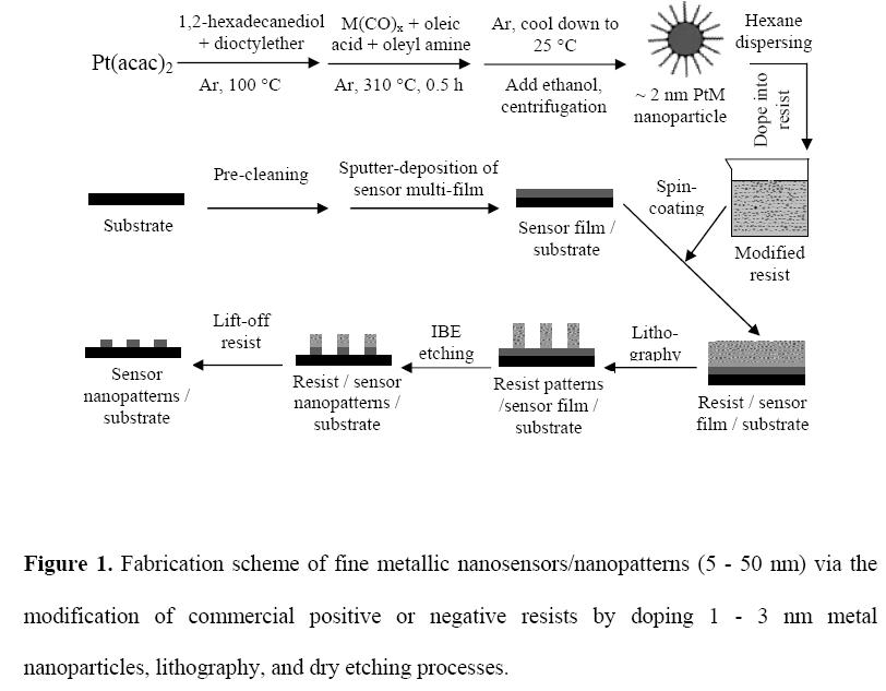
Using their semimetallic resists, the researchers created patterns with dimensions of 5–50 nanometers and in shapes that were at least twice as long as they were wide on a variety of substrate types including silicon and metal. “The high-resolution patterning is possible because the 1–3 nanometer metal particles can reduce resist charging during electron-beam exposure by increasing its conductivity, as well as increasing the resist strength and adhesion to the substrate,” explains Zong.
The researchers also demonstrated that the resists could be used to make the complex patterns required to fabricate magnetic tunnel junction nanosensors, which are used in the read heads of magnetic data storage devices. They were also able to make nanosensors as small as 13 nanometers wide. This level of miniaturization will be vital for the ultra-high-density data storage that is keenly sought by industry.
A General Approach to Semimetallic, Ultra-High-Resolution, Electron-Beam Resists
Commercial electron-beam resists are modified into semimetallic resists by doping with 1-3 nm metal nanoparticles, which improve the resolution, contrast, strength, dry-etching resistance, and other properties of the resist. With the modified resists, fine resist nanopatterns from electron-beam lithography are readily converted into 5-50 nm, high-quality multilayers for metallic nanosensors or nanopatterns via ion-beam etching. This method solves the problem of the fabrication of fine (
Brian Wang is a Futurist Thought Leader and a popular Science blogger with 1 million readers per month. His blog Nextbigfuture.com is ranked #1 Science News Blog. It covers many disruptive technology and trends including Space, Robotics, Artificial Intelligence, Medicine, Anti-aging Biotechnology, and Nanotechnology.
Known for identifying cutting edge technologies, he is currently a Co-Founder of a startup and fundraiser for high potential early-stage companies. He is the Head of Research for Allocations for deep technology investments and an Angel Investor at Space Angels.
A frequent speaker at corporations, he has been a TEDx speaker, a Singularity University speaker and guest at numerous interviews for radio and podcasts. He is open to public speaking and advising engagements.
