

Ad Support : Nano Technology Netbook Technology News Computer Software
The use of silicon nanowire transistors is proposed to allow the continued scaling of CMOS beyond what is possible in planar fabrication. This and the nanowires for memristors from HP means that Moore’s law will continue for at least 2 or 3 more decades.
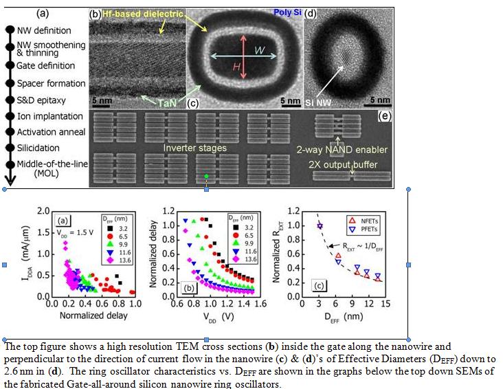
Link to the word document summary of the IBM paper Gate-all-around Silicon Nanowire 25-Stage CMOS Ring Oscillators with Diameter Down to 3 nm
As of today, the workhorse driving the ever increasing amount of computing power from PC’s to mobile phones has been the relentless scaling of the planar MOS transistor, however its continued scaling is approaching a brick wall and alternative solutions are required.
Scaling the device gate length is becoming increasingly challenging for traditional planar devices. Following the conventional scaling laws requires thinner gate dielectrics, shallower junctions and higher channel doping. All of these components are reaching the limit of what is physically possible. However, by moving from the planar architecture to a three-dimensional channel geometry, electrostatic control of the channel by the gate is improved and scaling can be further extended beyond the current limits. A near-term solution being evaluated by the industry is the FINFET device, which improves the electrostatic channel control by putting two gates on both sides of the fin channel. The ultimate evolution of this concept is a gate-all-around nanowire device, which is a silicon wire completely surrounded by a controlling gate. This geometry, therefore, provides the best possible electrostatic channel control. A research team at the IBM Microelectronic Research Lab at Yorktown Heights, NY, was able to produce the world’s first functional ring-oscillator circuits with the gate-all-around silicon nanowire devices, demonstrating that this type of device can yield complex circuits. The silicon wire diameter was made as small as 3 nm with gate lengths down to 25 nm. These results clearly demonstrate a viable scaling path for silicon-based devices.
The fabrication of ring oscillator structures made up from CMOS inverters demonstrates that this type of device can yield complex circuits.The silicon nanowire transistors have a hafnium-based dielectric layer separating the inner silicon wire from a gate-all-around polycrystalline silicon gate. The silicon wire was made with a range of diameters down to 2.6-nm and with gate lengths down to 25-nm. The nanowire capacitance shows a size dependence in agreement with that of a cylindrical capacitor and the ac characterization shows enhanced self-heating below diameters of 5-nm.
If you liked this article, please give it a quick review on Reddit, or StumbleUpon. Thanks
Supporting Advertising
Business Success
How to Make Money
Executive Jobs
Paid Surveys
Thank You

Brian Wang is a Futurist Thought Leader and a popular Science blogger with 1 million readers per month. His blog Nextbigfuture.com is ranked #1 Science News Blog. It covers many disruptive technology and trends including Space, Robotics, Artificial Intelligence, Medicine, Anti-aging Biotechnology, and Nanotechnology.
Known for identifying cutting edge technologies, he is currently a Co-Founder of a startup and fundraiser for high potential early-stage companies. He is the Head of Research for Allocations for deep technology investments and an Angel Investor at Space Angels.
A frequent speaker at corporations, he has been a TEDx speaker, a Singularity University speaker and guest at numerous interviews for radio and podcasts. He is open to public speaking and advising engagements.
