
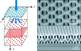
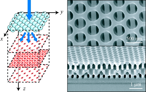
The new 3D nanofabrication method makes it possible to manufacture complex multi-layered solids all in one step. In this example, seen in these Scanning Electron Microscope images, a view from above (at top) shows alternating layers containing round holes and long bars. As seen from the side (lower image), the alternating shapes repeat through several layers. Image: Chih-Hao Chang
An MIT team has found a way to produce more complicated 3D nanostructures by using a blend of current “top-down” and “bottom-up” approaches. The new method is a hybrid in which the self-assembled array is produced directly on a substrate material, performing the function of a mask for the lithography process.
Nanoletters – From Two-Dimensional Colloidal Self-Assembly to Three-Dimensional Nanolithography
A number of “top-down” lithographic and “bottom-up” self-assembly methods have been developed to fabricate three-dimensional (3D) nanostructures to support the recent advances in nanotechnology. But they are limited by a number of factors such as fabrication cost, pattern resolution, and/or flexibility of geometry. Here we present a 3D nanolithography process that utilizes self-assembled nanospheres to create a periodic array of focal spots, which are then replicated across multiple depth in a transparent medium according to the Talbot effect. The Talbot field then exposes a pattern onto the underlying photoresist, recording the 3D intensity distribution. We have demonstrated designable complex 3D periodic structures with 80 nm minimum feature size, roughly one-fourth of the operating wavelength. This approach combines 2D colloidal self-assembly and 3D phase lithography, is robust, cost-effective, and widely applicable to nanoscale research and manufacturing.
One approach to making three-dimensional nanostructures — a top-down approach — is called phase-shift lithography, in which a two-dimensional mask shapes the intensity of light shining onto a layer of photoresist material (in the same way a photographic negative controls the amount of light reaching different areas of a print). The photoresist is altered only in the areas reached by the light. However, this approach requires very precisely manufactured phase masks, which are expensive and time-consuming to make.
Another method — a bottom-up approach — is to use self-assembling colloidal nanoparticles that form themselves into certain energetically favorable close-packed arrangements. These can then be used as a mask for physical deposition methods, such as vapor deposition, or etching of the surface, to produce 2-D structures, just as a stencil can be used to control where paint reaches a surface. But these methods are slow and limited by defects that can form in the self-assembly process, so although they can be used for the fabrication of 3-D structures, this is made difficult because any defects propagate through the layers.
“We do a little bit of both,” Chang says. “We took a chemist’s method and added in a flavor of engineering.”
The new method is a hybrid in which the self-assembled array is produced directly on a substrate material, performing the function of a mask for the lithography process. The individual nanoparticles that assemble on the surface each act as tiny lenses, focusing the beam into an intensity pattern determined by their arrangement on the surface. The method, the authors say in their paper, “can be implemented as a novel technique to fabricate complex 3-D nanostructures in all fields of nanoscale research.”
Depending on the shapes and arrangements of the tiny glass beads they use for the self-assembly part of the process, it is possible to create a great variety of structures, “from holes to higher-density posts, rings, flowery structures, all using the exact same system,” Chang says. “It’s a very simple way to make 3-D nanostructures, and probably the cheapest way right now. You can use it for many things.”
Team members, whose specialty is in optics, say the first structures they plan to make are photonic crystals, whose structure can manipulate the behavior of light beams passing through them. But the method can also be used to make phononic materials, which control waves of heat or sound, or even to make filters with precisely controlled porosity, which might have biomedical applications.

11 pages of supplemental material
If you liked this article, please give it a quick review on ycombinator or StumbleUpon. Thanks

Brian Wang is a Futurist Thought Leader and a popular Science blogger with 1 million readers per month. His blog Nextbigfuture.com is ranked #1 Science News Blog. It covers many disruptive technology and trends including Space, Robotics, Artificial Intelligence, Medicine, Anti-aging Biotechnology, and Nanotechnology.
Known for identifying cutting edge technologies, he is currently a Co-Founder of a startup and fundraiser for high potential early-stage companies. He is the Head of Research for Allocations for deep technology investments and an Angel Investor at Space Angels.
A frequent speaker at corporations, he has been a TEDx speaker, a Singularity University speaker and guest at numerous interviews for radio and podcasts. He is open to public speaking and advising engagements.