
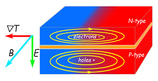
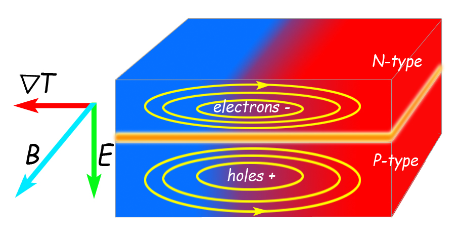
An n-type semiconductor on top of a p-type semiconductor creates a vertical electric field (E, green arrow), while diffusion creates a depletion layer near the junction (orange), where the electric field is strongest. Heating one end of the device creates a heat gradient at right angles to the electric field (del T, red arrow). Electrons and holes moving in these fields are forced into loops of current, and a magnetic field is generated “sideways” (B, blue arrow), at right angles to both electric and thermal fields.
Berkeley Lab scientists and their colleagues have discovered a new relation among electric and magnetic fields and differences in temperature, which may lead to more efficient thermoelectric devices that convert heat into electricity or electricity into heat. Berkeley Lab scientists find that uneven temperature can lead to electronic whirlpools and sideways magnetic fields. The new effect that has been discovered has been overlooked by the thermopower community, and can greatly affect the efficiency of thermopower and other devices.
Physical Review B – Electrothermally driven current vortices in inhomogeneous bipolar semiconductors
Wu and his colleagues found that temperature gradients in semiconductors, when one side of the device is hotter than the opposite side, can produce electronic vortices – whirlpools of electric current – and can, at the same time, create magnetic fields at right angles to both the plane of the swirling electric currents and the direction of the heat gradient. The researchers report their results in Physical Review B.
Wu says, “There are four well-known effects that relate thermal, electric, and magnetic fields” – for example, the familiar Hall effect, which describes the voltage difference across an electric conductor in a perpendicular magnetic field – “but in all these effects the magnetic field is an input, not an outcome. We asked, ‘Why not use the electric field and the heat gradient as inputs and try to generate a magnetic field?’”
To test the possibilities, the researchers modeled a practical device made of two layers of silicon: a thin, negatively doped layer (N-type) with an excess of electrons and a thicker, positively doped layer (P-type) with an excess of holes, which are electron absences that behave as positively charged particles.
At the junction where the oppositely doped silicon layers meet, a third kind of layer called a P-N junction forms, not physical but electronic: electrons from the N-type layer diffuse across the physical boundary into the P-type layer while holes move in the opposite direction, forming a depletion layer where charges are “dried out”.
Given the high density of mobile electrons at the surface of the N-type layer and the high density of mobile holes at the surface of the P-type layer, but few mobile charges in the depletion layer, the electric field is strongest near the junction. This deep layer has profound effects, when a heat gradient is applied to the joined silicon layers.
If you liked this article, please give it a quick review on ycombinator or StumbleUpon. Thanks

Brian Wang is a Futurist Thought Leader and a popular Science blogger with 1 million readers per month. His blog Nextbigfuture.com is ranked #1 Science News Blog. It covers many disruptive technology and trends including Space, Robotics, Artificial Intelligence, Medicine, Anti-aging Biotechnology, and Nanotechnology.
Known for identifying cutting edge technologies, he is currently a Co-Founder of a startup and fundraiser for high potential early-stage companies. He is the Head of Research for Allocations for deep technology investments and an Angel Investor at Space Angels.
A frequent speaker at corporations, he has been a TEDx speaker, a Singularity University speaker and guest at numerous interviews for radio and podcasts. He is open to public speaking and advising engagements.