

Recent Developments in 2G HTS Coil Technology (20 pages, Sept 19, 2011)
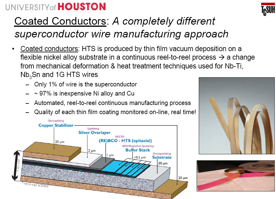
Coated Conductors: A completely different superconductor wire manufacturing approach
• Coated conductors: HTS is produced by thin film vacuum deposition on a flexible nickel alloy substrate in a continuous reel-to-reel process a change from mechanical deformation and heat treatment techniques used for Nb-Ti, Nb3Sn and 1G HTS wires
– Only 1% of wire is the superconductor
– ~ 97% is inexpensive Ni alloy and Cu
– Automated, reel-to-reel continuous manufacturing process
– Quality of each thin film coating monitored on-line, real time
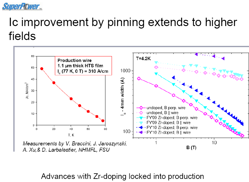
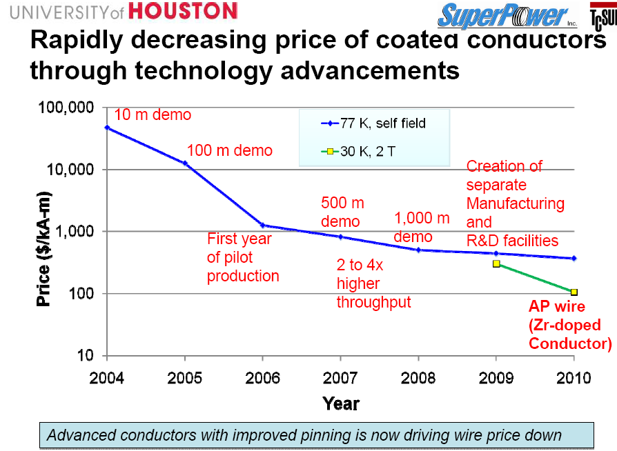
Long tapes with Zr-doping exhibit critical currents of over 250 A/cm in tapes run through the manufacturing facility at up to 1400 meter lengths.
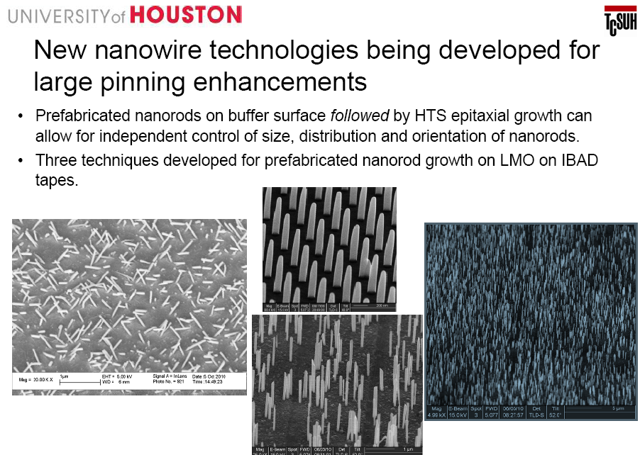
New nanowire technologies being developed for large pinning enhancements
• Prefabricated nanorods on buffer surface followed by HTS epitaxial growth can allow for independent control of size, distribution and orientation of nanorods.
• Three techniques developed for prefabricated nanorod growth on LMO on IBAD tapes.
Immense challenge in scaling up coated conductor fabrication from R and D to manufacturing
• Epitaxial thin film growth over kilometer
– Never been accomplished in any material system
• Uniform critical current over kilometer lengths
– Uniform stoichiometry of superconductor over kilometer lengths
– Uniform thickness of 5-layer buffer stack without imperfections (porosity, scratches…) over a kilometer with buffer thickness as small as 7 nm
• High-rate vapor deposition of complex, multi-component films over 1 μm in thickness over large deposition area.
• Stable deposition conditions over 40 hours with temperature, precursor deposition uniformity over 100 cm × 15 cm deposition area
Superconductors by 2016
Multiple opportunities available for large improvements: Intense R and D underway
• Plenty of opportunities for 10x improvement in production wire performance at low temperatures and high fields ==> 10x lower cost/performance
– 400 A/mm (4 MA/cm2) target for production wires in 2.5 μm thick films: 3x today’s capability
– 3x additional improvement lift factor in high magnetic fields at low and intermediate temperatures by enhanced pinning schemes
• Goal of Je = 6000 A/mm2 at 4.2 K, 15 T perpendicular to wire (~ 10x Nb3Sn performance); 6000 A/cm at 40 K, 3 T perpendicular to wire
• Scalable processes being developed for fully striated multfilamentary wires in long lengths for low ac losses ; ac loss reduction goal 5x (near term) to 30x
• 3x improvement in MOCVD process efficiency targeted using novel equipment engineering ==> 3x lower cost + 3x higher throughput
• Continued R and D for novel in-line process control and quality control for high yield manufacturing of long piece-length conductors.
Superior product configurations available now….
Expect Extraordinary and Universal product in the next five years.

If you liked this article, please give it a quick review on ycombinator or StumbleUpon. Thanks

Brian Wang is a Futurist Thought Leader and a popular Science blogger with 1 million readers per month. His blog Nextbigfuture.com is ranked #1 Science News Blog. It covers many disruptive technology and trends including Space, Robotics, Artificial Intelligence, Medicine, Anti-aging Biotechnology, and Nanotechnology.
Known for identifying cutting edge technologies, he is currently a Co-Founder of a startup and fundraiser for high potential early-stage companies. He is the Head of Research for Allocations for deep technology investments and an Angel Investor at Space Angels.
A frequent speaker at corporations, he has been a TEDx speaker, a Singularity University speaker and guest at numerous interviews for radio and podcasts. He is open to public speaking and advising engagements.