
Arxiv – A robust, scanning quantum system for nanoscale sensing and imaging
Controllable atomic-scale quantum systems hold great potential as sensitive tools for nanoscale imaging and metrology. Possible applications range from nanoscale electric and magnetic fi eld sensing to single photon microscopy, quantum information processing, and bioimaging. At the heart of such schemes is the ability to scan and accurately position a robust sensor within a few nanometers of a sample of interest, while preserving the sensor’s quantum coherence and readout fidelity. These combined requirements remain a challenge for all existing approaches that rely on direct grafting of individual solid state quantum systems or single molecules onto scanning-probe tips. Here, we demonstrate the fabrication and room temperature operation of a robust and isolated atomic-scale quantum sensor for scanning probe microscopy. Speci fically, we employ a high-purity, single-crystalline diamond nanopillar probe containing a single Nitrogen-Vacancy (NV) color center. We illustrate the versatility and performance of our scanning NV sensor by conducting quantitative nanoscale magnetic fi eld imaging and near-fi eld single-photon fluorescence quenching microscopy. In both cases, we obtain imaging resolution in the range of 20 nm and sensitivity unprecedented in scanning quantum probe microscopy.

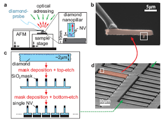
Experimental setup and probe fabrication for the scanning NV sensor. (a) Schematic of the setup consisting of a combined optical and atomic force microscope (AFM). We use a 532 nm laser (green arrows) to address the scanning NV center through its red fluorescence (red arrows). The scanning NV center resides in a diamond nanopillar (inset) and its proximity to the sample is maintained through AFM feedback. (b) Scanning electron microscope (SEM) image of a single-crystalline diamond nanopillar-probe (falsecolor coded in red) with a single NV center in its tip. (c) Brief depiction of the fabrication process for scanning single-crystalline diamond NV sensors. Electron-beam lithography is used to defi ne nanopillars and platforms from the top- and bottom-sides of a few micron thin diamond membrane. Patterns are then transferred to the diamond by reactive ion etching. (d) SEM image of a finalized array of diamond platforms with nanopillars. In all panels, dotted rectangles highlight diamond nanopillars.
The NV center in diamond is a point-defect that offers the potential for sensing and imaging with atomic scale resolution. Sensitive nanoscale detection of various physical quantities is possible because the NV center forms a bright and stable single photon source for optical imaging, and possesses a spin-triplet ground state which off ers excellent magnetic and electric fi eld sensing capabilities. The remarkable performance of the NV center in such spin-based sensing schemes, is the result of the long NV spin coherence time, combined with efficient optical spin preparation and readout, all at room temperature. In addition, NV centers can be positioned within nanometers of a diamond surface and therefore in close proximity of a sample to maximize signal strengths and spatial resolution. In order to realize the full potential of these attractive features, we have developed a “scanning NV sensor” (Fig. 1a), which employs a diamond nanopillar as the scanning probe, with an individual NV center arti ficially created within a few nanometers of the pillar tip through ion implantation. Long NV spin coherence times (about 30 microseconds) are achieved as our devices are fabricated from high purity, single-crystalline bulk diamond. Furthermore, diamond nanopillars are efficient waveguides for the NV fluorescence band], which yields record-high NV signal collection efficiencies for a scanning NV device.
Our scanning diamond nanopillars have typical diameter about 200 nm and length of 1 micron and are fabricated on few-micron sized diamond platforms which can be attached to atomic force microscope (AFM) tips for scanning.
We note that for magnetic fi eld imaging, our current ability to resolve individual
magnetic domains already equals the typical performance of alternative methods, with the added advantages of being non-invasive and quantitative. The magnetic field sensitivity we demonstrated with the scanning NV sensor compares well to the performance realized previously with single NV centers in ultrapure, bulk diamond samples. Combined with the mechanical robustness and durability of our diamond probes (up to several weeks of scanning with the same tip), our results constitute a signi cant advance in scanning quantum probe microscopy and demonstrate the advantage of our method over alternative approaches.The scope of applications of the scanning quantum probe described here goes far beyond imaging and sensing. For example, our nanoscopic, scannable single photon
source, could be used to controllably inject single plasmonic excitations into nanometallic structures at well-de fined locations, which would have broad impact
to the fi eld of nano-plasmonics. Additionally, our device forms an ideal platform to coherently couple the scanning NV spin to other spin systems such as P in Si, other NV centers, or carbon-based spin qubits, either by optical or magnetic coupling. Quantum information could thereby be transferred between a stationary qubit and our scanning NV center and from there to other qubit systems or single photons
If you liked this article, please give it a quick review on ycombinator or StumbleUpon. Thanks

Brian Wang is a Futurist Thought Leader and a popular Science blogger with 1 million readers per month. His blog Nextbigfuture.com is ranked #1 Science News Blog. It covers many disruptive technology and trends including Space, Robotics, Artificial Intelligence, Medicine, Anti-aging Biotechnology, and Nanotechnology.
Known for identifying cutting edge technologies, he is currently a Co-Founder of a startup and fundraiser for high potential early-stage companies. He is the Head of Research for Allocations for deep technology investments and an Angel Investor at Space Angels.
A frequent speaker at corporations, he has been a TEDx speaker, a Singularity University speaker and guest at numerous interviews for radio and podcasts. He is open to public speaking and advising engagements.