
A team of researchers working out of the University of California, Berkeley, has developed an entirely new class of two-dimensional semiconductor made of indium arsenide. Called quantum membranes, the new material has a band structure and can be turned from a bulk material to a two-dimensional one, simply by reducing its size.
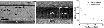
Nanoscale size effects drastically alter the fundamental properties of semiconductors. Here, we investigate the dominant role of quantum confinement in the field-effect device properties of free-standing InAs nanomembranes with varied thicknesses of 5–50 nm. First, optical absorption studies are performed by transferring InAs “quantum membranes” (QMs) onto transparent substrates, from which the quantized sub-bands are directly visualized. These sub-bands determine the contact resistance of the system with the experimental values consistent with the expected number of quantum transport modes available for a given thickness. Finally, the effective electron mobility of InAs QMs is shown to exhibit anomalous field and thickness dependences that are in distinct contrast to the conventional MOSFET models, arising from the strong quantum confinement of carriers. The results provide an important advance toward establishing the fundamental device physics of two-dimensional semiconductors.

Through detailed experiments and theoretical modeling, InAs QMs are presented as a model material system for elucidating the dominant role of the quantum confinement in the basic field-effect transport properties of carriers, including effective mobility and quantum resistance. InAs is specifically ideal for this study given the large Bohr radius which allows for heavy quantization at sub-20-nm thicknesses and the ease of Ohmic metal contact formation. Besides understanding the basic transport physics as a function of thickness, this work presents important practical implications for exploring the ultimate performance limits of ultrathin body InAs QM FETs, as well as providing guidelines for future device designs. Importantly, the contact resistance and mobility models inQMFETs are found to be drastically different than the previously established universal models for conventional MOSFETs, thereby presenting a new insight into the device physics of 2-D field-effect transistors. While InAs QMs were explored here, the results are generic for any structurally quantum confined material system.
If you liked this article, please give it a quick review on ycombinator or StumbleUpon. Thanks

Brian Wang is a Futurist Thought Leader and a popular Science blogger with 1 million readers per month. His blog Nextbigfuture.com is ranked #1 Science News Blog. It covers many disruptive technology and trends including Space, Robotics, Artificial Intelligence, Medicine, Anti-aging Biotechnology, and Nanotechnology.
Known for identifying cutting edge technologies, he is currently a Co-Founder of a startup and fundraiser for high potential early-stage companies. He is the Head of Research for Allocations for deep technology investments and an Angel Investor at Space Angels.
A frequent speaker at corporations, he has been a TEDx speaker, a Singularity University speaker and guest at numerous interviews for radio and podcasts. He is open to public speaking and advising engagements.