

1. University of Illinois researchers developed a method to chemically etch patterned arrays in the semiconductor gallium arsenide, used in solar cells, lasers, light emitting diodes (LEDs), field effect transistors (FETs), capacitors and sensors. Led by electrical and computer engineering professor Xiuling Li, the researchers describe their technique in the journal Nano Letters.
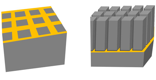
Metal-assisted chemical etching uses two steps. First, a thin layer of gold is patterned on top of a semiconductor wafer with soft lithography (left). The gold catalyzes a chemical reaction that etches the semiconductor form the top down, creating three-dimensional structures for optoelectronic applications (right).
Li and her group turned to metal-assisted chemical etching (MacEtch), a wet-etching approach they had previously developed for silicon. Unlike other wet methods, MacEtch works in one direction, from the top down. It is faster and less expensive than many dry etch techniques, according to Li. Her group revisited the MacEtch technique, optimizing the chemical solution and reaction conditions for the III-V semiconductor gallium arsenide (GaAs).
The process has two steps. First, a thin film of metal is patterned on the GaAs surface. Then, the semiconductor with the metal pattern is immersed in the MacEtch chemical solution. The metal catalyzes the reaction so that only the areas touching metal are etched away, and high-aspect-ratio structures are formed as the metal sinks into the wafer. When the etching is done, the metal can be cleaned from the surface without damaging it.
“It is a big deal to be able to etch GaAs this way,” Li said. “The realization of high-aspect-ratio III-V nanostructure arrays by wet etching can potentially transform the fabrication of semiconductor lasers where surface grating is currently fabricated by dry etching, which is expensive and causes surface damage.”
Next, the researchers hope to further optimize conditions for GaAs etching and establish parameters for MacEtch of other III-V semiconductors. Then, they hope to demonstrate device fabrication, including distributed Bragg reflector lasers and photonic crystals.
“MacEtch is a universal method as long as the right condition for deferential etching with and without metal can be found,” Li said.
A new generation of silicon computer chips, due to debut in 2012, will contain transistors having a vertical structure instead of a conventional flat design. However, because silicon has a limited “electron mobility” – how fast electrons flow – other materials will likely be needed soon to continue advancing transistors with this 3-D approach, Ye said.
Indium-gallium-arsenide is among several promising semiconductors being studied to replace silicon. Such semiconductors are called III-V materials because they combine elements from the third and fifth groups of the periodic table.
“Nanowires made of III-V alloys will get us to the 10 nanometer range,” he said.
The new findings confirmed that the device made using a III-V material has the potential to conduct electrons five times faster than silicon.
Creating smaller transistors also will require finding a new type of insulating layer essential for the devices to switch off. As gate lengths shrink smaller than 14 nanometers, the silicon dioxide insulator used in conventional transistors fails to perform properly and is said to “leak” electrical charge.
One potential solution to this leaking problem is to replace silicon dioxide with materials that have a higher insulating value, or “dielectric constant,” such as hafnium dioxide or aluminum oxide.
In the new work, the researchers applied a dielectric coating made of aluminum oxide using a method called atomic layer deposition. Because atomic layer deposition is commonly used in industry, the new design may represent a practical solution to the coming limits of conventional silicon transistors.
If you liked this article, please give it a quick review on ycombinator or StumbleUpon. Thanks

Brian Wang is a Futurist Thought Leader and a popular Science blogger with 1 million readers per month. His blog Nextbigfuture.com is ranked #1 Science News Blog. It covers many disruptive technology and trends including Space, Robotics, Artificial Intelligence, Medicine, Anti-aging Biotechnology, and Nanotechnology.
Known for identifying cutting edge technologies, he is currently a Co-Founder of a startup and fundraiser for high potential early-stage companies. He is the Head of Research for Allocations for deep technology investments and an Angel Investor at Space Angels.
A frequent speaker at corporations, he has been a TEDx speaker, a Singularity University speaker and guest at numerous interviews for radio and podcasts. He is open to public speaking and advising engagements.