

Wired – By 2017, HP hopes to build a computer chip that includes 256 microprocessors tied together with beams of light. Codenamed Corona, this laser-powered contraption would handle ten trillion floating points operations a second. In other words, if you put just five of them together, you’d approach the speed of today’s supercomputers. The chip’s 256 cores would communicate with each other at an astonishing 20 terabytes per second, and they’d talk to memory at 10 terabytes a second. That means it would run memory-intensive applications about two to six times faster than an equivalent chip made with good old fashioned electric wires.
Corona is just one of several efforts to build superfast chips that can bust through the exascale barrier, including Intel’s Runnemede, MIT’s Angstrom, NVIDIA’s Echelon,and Sandia’s X-calibur projects. All seek to use integrated photonics in some way, but the technology is the heart of the matter for HP’s 256-core Corona.
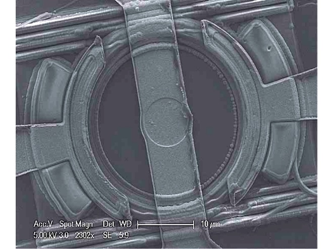
An electron microscope image of the “micro-ring photonic device” used by the Corona project (Photo: HP Labs)
A 12 page paper on the HP Corona chip (from ISCA 2008)
The aim is to build a tiny laser into each core, so that it can broadcast information to all other cores through an optical network. With even a minimal level of communication among processors, you can ensure uniform heat dissipation across the chip, and you can ramp clock speed up and down depending on workloads. This will not allow us to reach unprecedented speeds, it will significantly reduce power consumption.
Using electronics for a 10 terabytes per second channel between a CPU and external memory would require 160 watts of power. But HP Labs researchers calculate that using integrated photonics lowers that to 6.4 watts. (25 times more energy efficient)
MIT’s Kimerling recently came up with a new approach: germanium for onchip lasers. The material produces a laser that emits light at the wavelength used by communications networks, it operates at up to 120°C and germanium can be readily grown on silicon.
Kimerling coordinates an industry technology roadmap for integrated photonics at MIT. He says the timeframes companies are giving for when they need the technology have shrunk by about three years over the past year. “Many people said 2017,” says Kimerling. “Now it’s 2013, and we’ll take it today if you can give it to us.”
According to Kimerling, major semiconductor fab will be turning out integrated silicon photonic products later this year. The products are likely to be simple transceivers, but it shows that photonics is rapidly becoming a standard part of the chipmaking toolkit

Communication challenge in ultradense computing devices. Chips are not full speed because communication is not fast enough.
DARPA MoleApps–Aim: 10^15devices/ cm^3
2008 : 17 nm half-pitch,3.5*10^11 /cm2 demonstrated

Communication speed of 80 TB/s for full speed 2017 chips

Energy of Computing in 2005

If you liked this article, please give it a quick review on ycombinator or StumbleUpon. Thanks

Brian Wang is a Futurist Thought Leader and a popular Science blogger with 1 million readers per month. His blog Nextbigfuture.com is ranked #1 Science News Blog. It covers many disruptive technology and trends including Space, Robotics, Artificial Intelligence, Medicine, Anti-aging Biotechnology, and Nanotechnology.
Known for identifying cutting edge technologies, he is currently a Co-Founder of a startup and fundraiser for high potential early-stage companies. He is the Head of Research for Allocations for deep technology investments and an Angel Investor at Space Angels.
A frequent speaker at corporations, he has been a TEDx speaker, a Singularity University speaker and guest at numerous interviews for radio and podcasts. He is open to public speaking and advising engagements.