


Twin Creeks Technologies website provides details on the technology and economics of their process.
Siva Sivaram, the CEO of Twin Creeks, says the company’s technology both reduces the amount of silicon needed and the cost of the manufacturing equipment. He claims the company can produce solar cells for about 40 cents per watt, which compares to roughly 80 cents for the cheapest solar cells now. Twin Creeks has raised $93 million in venture capital, plus loans from the state of Mississippi and other sources that it used to build its solar factory.
The conventional way to make the crystalline silicon wafers—which account for the bulk of solar cells—involves cutting blocks or cylinders of silicon into 200-micrometer-thick wafers, a process that turns about half of the silicon into waste. The industry uses 200-micrometer wafers because wafers much thinner than that are brittle and tend to break on the manufacturing line. But in theory, they could be as thin as 20 to 30 micrometers and still be just as efficient, or more efficient, at converting sunlight into electricity.
Twin Creeks’s process makes 20-micrometer-thick wafers largely without waste. It involves applying a thin layer of metal that makes them durable enough to survive conventional solar-cell processing equipment. Sivaram says that by greatly reducing the use of wire saws and related equipment and making thinner wafers, Twin Creeks reduces the amount of silicon needed by 90 percent and also greatly reduces capital costs. He says the technology can be added to existing production lines. The company’s primary plan is to sell manufacturing equipment, rather than produce solar cells. “I expect that by this time next year, we’ll have a half a dozen to a dozen of these tools in the field,” he says.

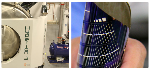
Accelerating solar power: Twin Creeks’s Hyperion 3 is an ion accelerator that bombards plates of silicon with hydrogen ions to produce very thin solar wafers for solar cells. The silicon plates are arranged around the outside of the spoke structure, which spins as the wafers are hit with ions.
Twin Creeks
The process begins in a vacuum chamber, where a high-energy beam of hydrogen ions bombards three-millimeter-thick disks of crystalline silicon. The ions accumulate at a precise depth of 20 micrometers, which is controlled by the voltage of the beam. Once enough ions accumulate, a robotic arm quickly removes the wafers, which are then placed inside a furnace, where the ions in the silicon form microscopic bubbles of hydrogen gas that expand, creating tiny fractures within the silicon wafer and causing a 20-micrometer-thick layer of silicon to flake off. The company then applies a metal backing to the thin silicon. (The proprietary process it uses sets it apart from another company, Astrowatt, which makes wafers that are similarly thin. But Astrowatt’s wafers are slightly curved, which could make them difficult to handle in conventional production equipment.)
The Twin Creeks wafers are compatible with conventional solar-cell production equipment, and with processes now being used to make advanced solar-cell designs, such as heterojunction cells. Sivaram says the hydrogen-ion process works with single-crystal materials other than silicon, including gallium arsenide, a semiconductor that has been used to produce world-record efficiency solar cells.
Using an ion beam to create thin wafers of crystalline silicon has been considered before, but it was far too expensive to be a practical manufacturing method. It required a particle accelerator that could produce ion beams that are both very high current and very high energy, and “such a beast did not exist,” Sivaram says. To make the technology viable, Twin Creeks developed an ion accelerator that is “10 times more powerful” than any commercially available accelerator, he says.
Hyperion, a manufacturing system developed by Twin Creeks Technologies, solves the problem of thick wafers with a technique called Proton Induced Exfoliation (PIE). In PIE, high-energy protons (or hydrogen ions) are embedded into “donor” wafers — standard wafers of silicon, germanium or other single-crystal materials— where they form a uniform layer beneath the surface of the donor. The physical attributes of hydrogen, combined with the conditions created by Hyperion, permit the ions to penetrate the surface of the donor wafer without changing its inherent properties and characteristics.
A single donor wafer can be reused repeatedly to create multiple laminae. Twin Creeks has lifted 14 laminae from a single donor wafer in its labs with Hyperion and produced solar cells on ten laminae lifted from a single donor wafer.
Hyperion has the potential to make your single-crystal wafer facilities up to 90% more efficient and reduce your demand for other wafer manufacturing equipment. A solar-factory based around Hyperion can produce cells for less than 40 cents a watt, or nearly half of the price of conventional systems today.
For semiconductor manufacturers, Hyperion can dramatically reduce the back-grinding and wafer thinning process steps in CMOS sensors and 3D packaging operations. With Hyperion, you can design a factory to suit the needs of the semiconductors being produced, not the mechanical shortcomings of conventional wafers.
Although others have experimented with producing thin wafers, Hyperion is the only production-ready system that can produce thin lamina in volume today. The system works because it operates at high voltage and high current, an unusual combination. High voltages are essential for deeply embedding ions while high current is important for the high throughput needed in modern manufacturing.
A single Hyperion 3 system, our commercial-scale manufacturing tool, can process over 1.5 million thin wafers per year, enough for more than 6 megawatts worth of solar cells. While Twin Creeks will initially concentrate on silicon wafers, Hyperion can be employed to produce thin crystalline wafers made from gallium arsenide, germanium, and other materials.
Complete Hyperion 3 systems are available for shipment.
Silicon, GaN, Germanium and More
While Hyperion will first be deployed to reduce the cost of silicon solar modules, Proton Induced Exfoliation is compatible with wafers made from other monocrystalline materials like germanium and silicon carbide. As a result, semiconductor manufacturers from a wide spectrum of the industry will adopt Hyperion for a variety of applications, including light emitting diodes, power electronics, CMOS sensors, 3D packaging and concentrated photovoltaics.
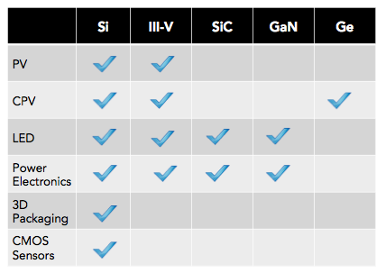
Reduced Cell Manufacturing Costs – Solar cells produced with Hyperion thin Si processing are nearly 50% less expensive to manufacture.
Reduced Capital Expenses – Hyperion makes your existing investments in polysilicon, ingot growing and wafering equipment up to 90% more efficient. If you need to expand, you can count on a 50% reduction in capital to make the same number of wafers.
Predictable Si costs – By consuming fewer materials per module, manufacturers are less exposed to swings in commodity prices. Manufacturers can better insulate themselves from fluctuations in spot and contract prices for silicon and other materials.
Flexible Format Cells – Solar modules produced with Hyperion thin Si lamina are bendable, allowing manufacturers to package solar directly into roofing materials to reduce packaging, installation and shipping costs.
If you liked this article, please give it a quick review on ycombinator or StumbleUpon. Thanks

Brian Wang is a Futurist Thought Leader and a popular Science blogger with 1 million readers per month. His blog Nextbigfuture.com is ranked #1 Science News Blog. It covers many disruptive technology and trends including Space, Robotics, Artificial Intelligence, Medicine, Anti-aging Biotechnology, and Nanotechnology.
Known for identifying cutting edge technologies, he is currently a Co-Founder of a startup and fundraiser for high potential early-stage companies. He is the Head of Research for Allocations for deep technology investments and an Angel Investor at Space Angels.
A frequent speaker at corporations, he has been a TEDx speaker, a Singularity University speaker and guest at numerous interviews for radio and podcasts. He is open to public speaking and advising engagements.