

Paul Scherrer Institute (PSI) researchers have investigated how they could make the semiconductor Germanium emit laser light. As a laser material, Germanium together with Silicon could form the basis for innovative computer chips in which information would be transferred partially in the form of light. This technology would revolutionise data streaming within chips and give a boost to the performance of electronics. The researchers have demonstrated that Germanium must be put under strain by an external force in order to turn it into a laser material.
Low energy and highly efficient onchip photonic communications is a key technology to enable zettaflop supercomputers
Direct-gap gain up to 850 cm-1 at 0.74 eV is measured and modeled in optically pumped Ge-on-Si layers for photoexcited carrier densities of 2.0×1020 cm-3. The gain spectra are correlated to carrier density via plasma-frequency determinations from reflection spectra. Despite significant gain, optical amplification cannot take place, because the carriers also generate pump-induced absorption of ≈7000 cm-1. Parallel studies of III–V direct-gap InGaAs layers validate our spectroscopy and modeling. Our self-consistent results contradict current explanations of lasing in Ge-on-Si cavities
Tiny Germanium Lasers should make Chips faster
Sigg’s research team, together with colleagues from the ETH Zurich and the Politecnico di Milano, has now been able to demonstrate that Germanium, under certain conditions, can function as a laser material. “Germanium lasers could make a break-through possible here, because Germanium can be readily combined with Silicon, which is the basic material from which chips are made. Silicon itself cannot emit light and can hardly be combined with any available laser material”, points out Sigg.
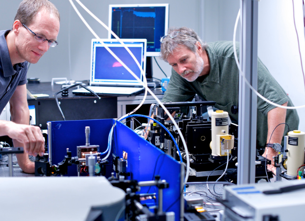
In their studies, which were performed at the Swiss Light Source (SLS) at PSI, the researchers investigated those properties of Germanium that are important for the generation of laser light, and compared them with those of currently available laser materials. “We stimulate the material by means of a powerful laser and simultaneously observe the changes occurring using infra-red radiation from the SLS”, elucidates the doctoral student Peter Friedli, who carried out the decisive experiments together with scientist Lee Carroll. “To do this, we used the fact that these light pulses are only 100 picoseconds (i.e. 0.1 billionths of a second) long, allowing us to follow the relevant processes in the material; that is, the behaviour of electrons at different points in time.”
If you liked this article, please give it a quick review on ycombinator or StumbleUpon. Thanks

Brian Wang is a Futurist Thought Leader and a popular Science blogger with 1 million readers per month. His blog Nextbigfuture.com is ranked #1 Science News Blog. It covers many disruptive technology and trends including Space, Robotics, Artificial Intelligence, Medicine, Anti-aging Biotechnology, and Nanotechnology.
Known for identifying cutting edge technologies, he is currently a Co-Founder of a startup and fundraiser for high potential early-stage companies. He is the Head of Research for Allocations for deep technology investments and an Angel Investor at Space Angels.
A frequent speaker at corporations, he has been a TEDx speaker, a Singularity University speaker and guest at numerous interviews for radio and podcasts. He is open to public speaking and advising engagements.