

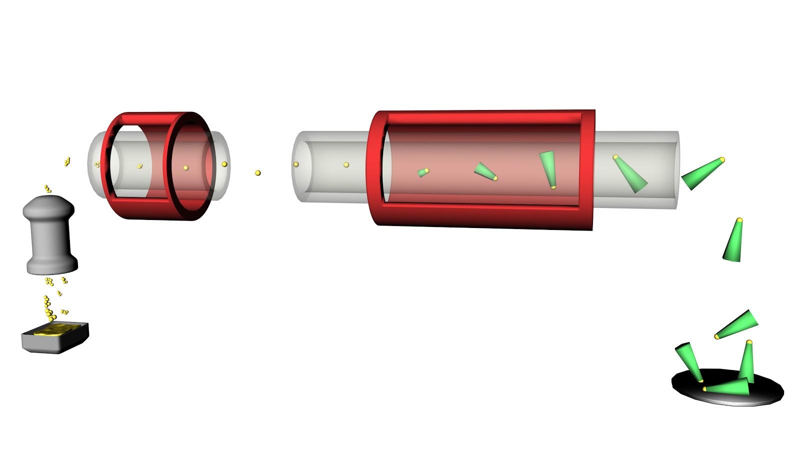
A completely new method of manufacturing the smallest structures in electronics could make their manufacture thousands of times quicker, allowing for cheaper semiconductors. Instead of starting from a silicon wafer or other substrate, as is usual today, researchers have made it possible for the structures to grow from freely suspended nanoparticles of gold in a flowing gas.
They believe the technology will be ready for commercialisation in two to four years’ time. A prototype for solar cells is expected to be completed in two years.
“When I first suggested the idea of getting rid of the substrate, people around me said ‘you’re out of your mind, Lars; that would never work’. When we tested the principle in one of our converted ovens at 400°C, the results were better than we could have dreamt of”, he says.
“The basic idea was to let nanoparticles of gold serve as a substrate from which the semiconductors grow. This means that the accepted concepts really were turned upside down!”
Since then, the technology has been refined, patents have been obtained and further studies have been conducted. In the article in Nature, the researchers show how the growth can be controlled using temperature, time and the size of the gold nanoparticles.
Nature – Continuous gas-phase synthesis of nanowires with tunable properties.
They have also built a prototype machine with a specially built oven. Using a series of ovens, the researchers expect to be able to ‘bake’ the nanowires, as the structures are called, and thereby develop multiple variants, such as p-n diodes.
A further advantage of the technology is avoiding the cost of expensive semiconductor wafers.
“In addition, the process is not only extremely quick, it is also continuous. Traditional manufacture of substrates is batch-based and is therefore much more time-consuming”, adds Lars Samuelson.
At the moment, the researchers are working to develop a good method to capture the nanowires and make them self-assemble in an ordered manner on a specific surface. This could be glass, steel or another material suited to the purpose.
The reason why no one has tested this method before, in the view of Professor Samuelson, is that today’s method is so basic and obvious. Such things tend to be difficult to question.However, the Lund researchers have a head start thanks to their parallel research based on an innovative method in the manufacture of nanowires on semiconductor wafers, known as epitaxy – consequently, the researchers have chosen to call the new method aerotaxy. Instead of sculpting structures out of silicon or another semiconductor material, the structures are instead allowed to develop, atomic layer by atomic layer, through controlled self-organisation.
ABSTRACT – Semiconductor nanowires are key building blocks for the next generation of light-emitting diodes, solar cells and batteries. To fabricate functional nanowire-based devices on an industrial scale requires an efficient methodology that enables the mass production of nanowires with perfect crystallinity, reproducible and controlled dimensions and material composition, and low cost. So far there have been no reports of reliable methods that can satisfy all of these requirements. Here we show how aerotaxy, an aerosol-based growth method, can be used to grow nanowires continuously with controlled nanoscale dimensions, a high degree of crystallinity and at a remarkable growth rate. In our aerotaxy approach, catalytic size-selected Au aerosol particles induce nucleation and growth of GaAs nanowires with a growth rate of about 1 micrometre per second, which is 20 to 1,000 times higher than previously reported for traditional, substrate-based growth of nanowires made of group III–V materials. We demonstrate that the method allows sensitive and reproducible control of the nanowire dimensions and shape—and, thus, controlled optical and electronic properties—through the variation of growth temperature, time and Au particle size. Photoluminescence measurements reveal that even as-grown nanowires have good optical properties and excellent spectral uniformity. Detailed transmission electron microscopy investigations show that our aerotaxy-grown nanowires form along one of the four equivalent 111B crystallographic directions in the zincblende unit cell, which is also the preferred growth direction for III–V nanowires seeded by Au particles on a single-crystal substrate. The reported continuous and potentially high-throughput method can be expected substantially to reduce the cost of producing high-quality nanowires and may enable the low-cost fabrication of nanowire-based devices on an industrial scale.
If you liked this article, please give it a quick review on ycombinator or StumbleUpon. Thanks

Brian Wang is a Futurist Thought Leader and a popular Science blogger with 1 million readers per month. His blog Nextbigfuture.com is ranked #1 Science News Blog. It covers many disruptive technology and trends including Space, Robotics, Artificial Intelligence, Medicine, Anti-aging Biotechnology, and Nanotechnology.
Known for identifying cutting edge technologies, he is currently a Co-Founder of a startup and fundraiser for high potential early-stage companies. He is the Head of Research for Allocations for deep technology investments and an Angel Investor at Space Angels.
A frequent speaker at corporations, he has been a TEDx speaker, a Singularity University speaker and guest at numerous interviews for radio and podcasts. He is open to public speaking and advising engagements.