

There was an Atomically Precise, No Interface, Device Regime Workshop in the middle of 2012
The workshop was to explore the possibilities for novel devices and devices with improved performance in the evolving device regime being explored by the seminal work of Michelle Simmons and others. This new device regime creates metallic conductor, semiconductor, and insulator regions by deterministic and atomic precision placement of dopant atoms in Si, without metal-oxide-semiconductor interfaces.
Single electron, quantum dot, and single atom transistors, as well as 4 atom wide nanowires, and extremely low noise operation have already been demonstrated. The intention of the workshop was to gather some of the world’s leading device and atomic precision fabrication experts to explore new possibilities in the quantum computing, digital, and analog device areas and the improvements and extensions of atomic resolution processes, fabrication tools, and modeling/design tools that would be required to enable these new devices.
Recent work at the University of New South Wales in Sydney Australia in the group of Michelle Simmons has shown that it is possible to make transistors in a device regime that is dramatically different than is used for current semiconductor devices.
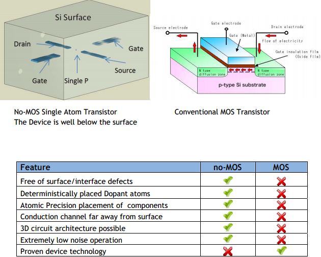
Using Scanning Tunneling Microscope (STM) lithography and dosing with phosphine, Phosphorous atoms (N-Type Dopants) can be placed by design (both number and position) in the silicon lattice. The device is overgrown with crystalline Si using Molecular Beam Epitaxy and is completely embedded in the silicon. In this way, a number of devices have been made without metal or oxide including a single atom transistor as shown in the figure. In other words this is not a Metal-Oxide-Semiconductor (MOS) device. For comparison, a schematic of a conventional MOSFET device is also shown. The table points to some advantages of this new no-MOS device regime that avoids some of the problems that limit conventional devices.
The principal conclusions of the workshop are:
* The atomic resolution and precision of STM patterning technology and the lack of heterogeneous materials interfaces for patterns of P dopants in Si have already
demonstrated unprecedented advantages to realize components of a quantum computing
technology, conducting nanowires, downscaled quantum dot devices, and low noise
performance.
Significant improvements in this technology could be realized by:
o improving the accuracy and throughput of tip based lithography
o increasing the variety of species of dopant atoms that can be placed
o extending the atomic precision placement of dopants to the third dimension.
* Modeling and simulation at the atomic scale on extended device structures is critical for device design, performance optimization, and aspects of metrology.
* Scalable quantum computing may not be obtainable without atomic precision placement.
* Classical digital and analog devices could be improved or developed in this regime.
Classes of devices presently being pursued, and the specific benefits of this technology, include:
* Single P atom Multi Qubit devices (both spin and charge qubits).
o More control over qubit characteristics through accurate dopant atom placement
o Expanded design space with 3D electrode placement
o Better control of individual qubits by screening fields with acceptor dopants
* Resonant tunneling quantum dot devices for digital applications.
o Improved On/Off ratio through atomically abrupt dopant profiles
o Deterministic control of electronic states in quantum dots
o Expanded design space with 3D electrode placement
* Tunnel FET for digital applications
o Much sharper donor/acceptor profiles leads to superior performance
o No interface traps or etch-induced line edge roughness
Other areas that would gain advantage from this approach
* Nano magnetic spin devices
o Magnetic dopants or nanowire inductors for spin control
* Analog RF amplifiers, sense amps, A/D & D/A converters
o Dramatic reduction in noise would aid analog applications
* Metamaterial Devices
o Metallic-like nanowires that can be patterned to arbitrary shapes in 3D may offer new avenues for nanoplasmonic and nanophotonic devices.
Device Ideas:
The ability to place dopant atoms with atomic precision as developed by the Simmons group, in three dimensions in Si and/or Ge has a number of significant advantages for electronic devices that span analog, classical digital information, and quantum information processing devices. The fact that metallic conducting, semiconducting, and insulating regions can be produced with extremely sharp boundaries, in an area that has effectively no material boundaries has a number of significant advantages that may be exploited.
With no metal oxide semiconductor (MOS) interfaces there are none of the associated
defects, charge traps, or interfacial roughness to introduce noise or degrade device performance
Atomically precise control over the number of dopant atoms and their placement allows unprecedented control of the energy levels in quantized structures (such as quantum dots) and the level of interaction between these quantized energy levels. This should lead to more predictable and reliable device performance.
During the workshop several presenters mentioned some of the limitations of planar
architectures when placing control and readout electrodes required for desired operations.
The ability to place dopant atoms with atomic precision in three dimensions would avoid many of these limitations.
Improvements in atomic precision fabrication can be applied to aspects of conventional MOS device architectures, for instance deterministic placement of dopants in channels, or atomically defined volumes of pure Si.
The participants of the workshop identified several classes of electronic devices that could
benefit from this new device regime made possible by emerging atomic resolution processing.
They are listed below:
A. P in Si Quantum Computing Devices
While there are many routes to quantum computing, the expected level of required redundancy suggests that reasonable levels of integration will be required to produce quantum computing systems that are practical. This demands that quantum computing devices and architectures need to be scalable with respect to the number of qubits in a computing system, and needs to be integrable into a conventional CMOS architecture. For this and many other reasons, the P in Si (and Ge) approach being pursued by the Simmons group appears to be one of the most attractive, as it is supported by existing semiconductor processing technology.
While single ion implantation for placement of individual P dopants has yielded some interesting results, the inevitable uncertainty in position due to limited spatial resolution in position of ion impact and straggle of ion trajectory after implant will simply not support the required precision in placement of the P atoms. Rahman explicitly made this point in his presentation. This leaves H depassivation lithography, phosphine dosing, and epitaxial overgrowth as the consensus approach for building P in Si quantum computing devices. This technique alone is the only one that can place P atoms accurately enough to have them interact effectively as either spin or charge qubits.
B. Atomic Precision Tunneling Field Effect Transistors (TFET)
In his presentation, Frank Register pointed out that TFETs have been identified as a very promising device for future technology nodes, but band tailing effects have limited the performance of these devices. With atomic precision placement of both N and P type dopants giving extremely sharp PN junctions, combined with three dimensional arrangement of gate electrodes, tunnel FETs fabricated with these approaches should have superior performance.
Klimeck and Rahman concluded that the extremely sharp P-N junctions were something that can be modeled with their simulation software NEMO in a very short period of time. This simulation will be included in one of the post-workshop reports.
C. NO MOS low noise analog amplifiers
D. Resonant tunneling devices with improved On/Off ratio
E. Magnetic impurities
F. Optical devices
G. Dangling bond as quantum dot devices
H. Enhanced crossbar QCA and CMOL architectures
I. Engineered nucleation sites for metal oxide crossbar switches
J. Single electron pumps
K. Si terahertz lasers
L. Medical devices
M. Strain sensitive devices
If you liked this article, please give it a quick review on ycombinator or StumbleUpon. Thanks

Brian Wang is a Futurist Thought Leader and a popular Science blogger with 1 million readers per month. His blog Nextbigfuture.com is ranked #1 Science News Blog. It covers many disruptive technology and trends including Space, Robotics, Artificial Intelligence, Medicine, Anti-aging Biotechnology, and Nanotechnology.
Known for identifying cutting edge technologies, he is currently a Co-Founder of a startup and fundraiser for high potential early-stage companies. He is the Head of Research for Allocations for deep technology investments and an Angel Investor at Space Angels.
A frequent speaker at corporations, he has been a TEDx speaker, a Singularity University speaker and guest at numerous interviews for radio and podcasts. He is open to public speaking and advising engagements.