

IM Flash Technologies LLC, the joint venture between Intel and Micron Technologies, is considering how and when to take its NAND flash memory ICs into the third dimension but reckons its development of a 20-nm memory cell has bought it a generation or two of 2-D scaling.
An industry-wide transition for the nonvolatile NAND flash memory technology from memory cells in a 2-D array to strings of NAND transistors integrated monolithically in the vertical direction is now anticipated. These 3-D memories are expected to be arranged as a 2-D array of vertical semiconductor channels with many levels of gate-all-around (GAA) structures forming the multiple voltage level memory cell transistors.
Toshiba is leading the charge towards 3-D NAND processes with its p-BiCS (pipe-shaped Bit Cost Scalable) technology, which it has presented at numerous learned conferences over several years. Towards the end of last year Toshiba announced that it had 16-layer devices based on a 50-nm diameter vertical channel. Samples are due this year and volume production in 2015. Toshiba’s p-BiC technology arranges the transistor string in a U-shape.
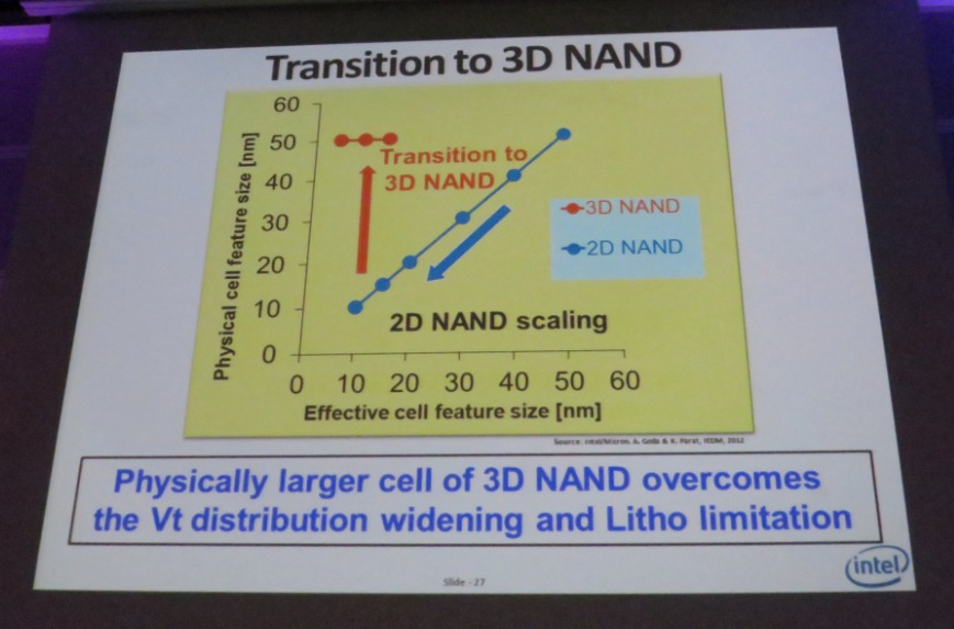
But Esfarjani, while acknowledging there is a scaling limit for 2-D NAND flash, indicated in one of his slides that 2-D NAND flash can scale to two more nodes at about 15- and 10-nm. The slide showed that the first 3-D NAND generation is likely to be brought up alongside that 15-nm 2-D node. Esfarjani added that 16 layer NAND flash ICs will not be enough to provide an economic benefit. “You need 64 or at least 32 layers,” he said.
Esfarjani said that the planar floating-gate high-K metal gate cell introduced by IMFT at the 20-nm node to replace a “wrap-around” cell used at 34- and 25-nm would scale further. IMFT introduced a 128-Gbit NAND flash memory at the 20-nm during 2012 (see Intel, Micron offer 128-Gbit NAND flash memory) leveraging its HKMG experience gained in logic circuits.
Among the techniques being used to extend the 2-D NAND flash generation are the addition of a nitride film and nanodots, said Esfarjani. “But a working cell is not enough. You also need high endurance of 10^5 cycles and higher,” he told the IMEC Technology Forum audience.
“The transition to 3-D is not limited by lithography,” Esfarjani said indicating that a 40-nm diameter semiconductor channel was about right. The challenges are in metrology, in finding materials that can withstand the temperatures of multilayer semiconductor processing and the high aspect ratio etch to drive in the vertical channel. This has to be controlled at an angle of taper of precisely 89.8 degrees, Esfarjani said.
“The NAND market will be with us and growing for years to come. 2-D NAND continues with the planar floating gate cell and 3-D NAND will carry us beyond the 10-nm limit,” concluded Esfarjani.
During questions at the end of his talk Esfarjani was asked if he could share information about the materials that IMFT is using to create the dielectric and gates within the vertical channel. He confirmed that IMFT is working on new materials but said that some information is too good to share.
If you liked this article, please give it a quick review on ycombinator or StumbleUpon. Thanks

Brian Wang is a Futurist Thought Leader and a popular Science blogger with 1 million readers per month. His blog Nextbigfuture.com is ranked #1 Science News Blog. It covers many disruptive technology and trends including Space, Robotics, Artificial Intelligence, Medicine, Anti-aging Biotechnology, and Nanotechnology.
Known for identifying cutting edge technologies, he is currently a Co-Founder of a startup and fundraiser for high potential early-stage companies. He is the Head of Research for Allocations for deep technology investments and an Angel Investor at Space Angels.
A frequent speaker at corporations, he has been a TEDx speaker, a Singularity University speaker and guest at numerous interviews for radio and podcasts. He is open to public speaking and advising engagements.