
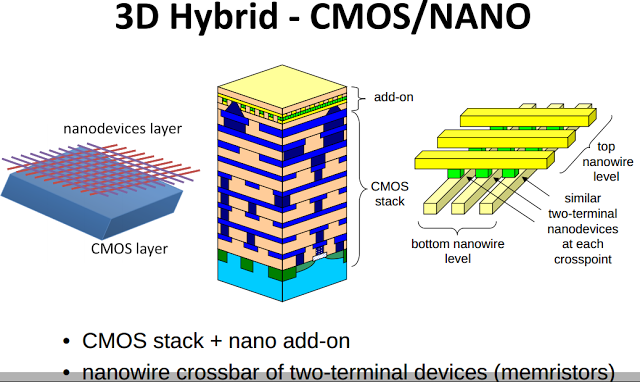
There is work towards creating 3D CMOs memristor circuits
Maximum Number of Layers
• Each layer has N^2 cells.
• There are r^2– 1 cross points per cell.
• That gives us a total of N^2 * (r^2 – 1) cross points per layer.
• The double decoding scheme allows us to address up to N^4 locations
• Which means that we can (potentially) have up to N^2 /(r^2 – 1) crossbar layers.
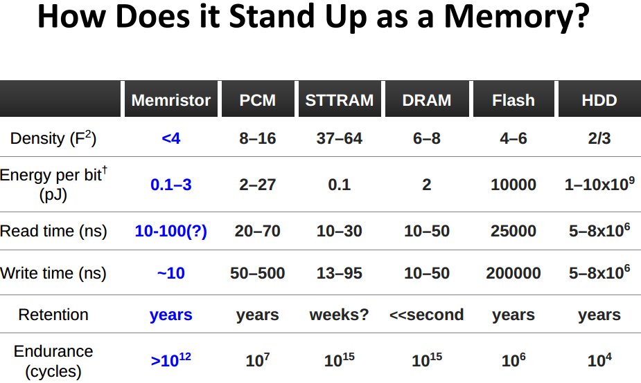
If Successful, 3D Hybrids Can Achieve…..
• Unprecedente dmemory density
– Footprint of a nano‐device is 4F nano 2/K, for K vertically integrated crossbar layers
– Potentially up to 10^14 bits on a single 1‐cm^2 chip
• Enormous memory bandwidth
– Potentially up to 10^18 bits/second/cm2
• At manageable power dissipation
• With abundant redundancy for yield/reliability

If you liked this article, please give it a quick review on ycombinator or StumbleUpon. Thanks

Brian Wang is a Futurist Thought Leader and a popular Science blogger with 1 million readers per month. His blog Nextbigfuture.com is ranked #1 Science News Blog. It covers many disruptive technology and trends including Space, Robotics, Artificial Intelligence, Medicine, Anti-aging Biotechnology, and Nanotechnology.
Known for identifying cutting edge technologies, he is currently a Co-Founder of a startup and fundraiser for high potential early-stage companies. He is the Head of Research for Allocations for deep technology investments and an Angel Investor at Space Angels.
A frequent speaker at corporations, he has been a TEDx speaker, a Singularity University speaker and guest at numerous interviews for radio and podcasts. He is open to public speaking and advising engagements.