

Precision Materials to Meet Scaling Challenges Beyond 14nm (18 pages)
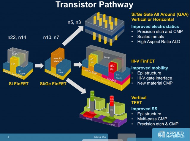
Beyond 14nm, as we move to 10 and 7nm, a new fin material will be required — probably silicon-germanium (SiGe), or perhaps just pure germanium.
SiGe will take us to 7nm then a new transistor structure is needed at 5 nanometers.
FinFET created a larger surface area, mitigating the effects of quantum tunneling, both Gate All Around (GAA) FETs and vertical tunneling FETs (TFETs), would again allow for shorter gates and lower voltages
A Gate All Around essentially consists of nanowire source and drains, surrounded by a gate. A vertical TFET is similar in that it uses nanowires, but the actual method of operation is very different from conventional FETs
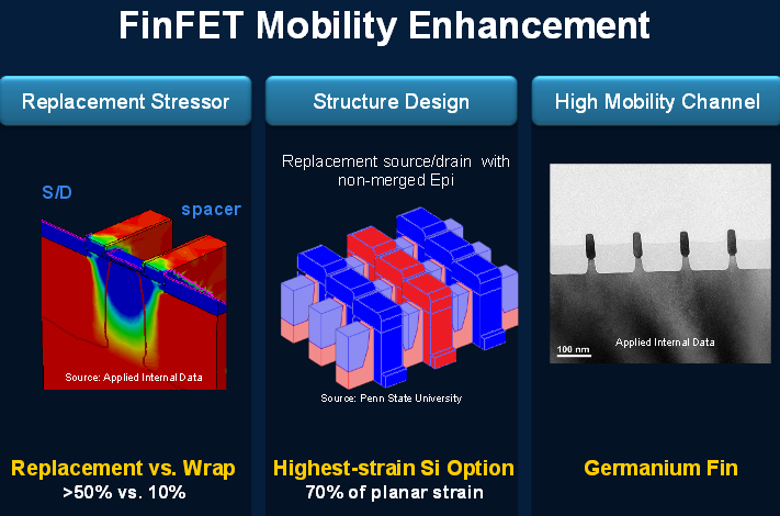
Precise control of materials is needed to deliver the required structure.
FinFET scaling requires precision control of materials
* CMP: precision through in-situ process control
* Dielectrics: composition tuning
* Junction: optimized activation
* Metal gate: multi Vt by metal gate composition and implant
* Metal gate: improved materials to control resistance at scaled CD
* Contact: optimized surface doping with implant + laser anneal
If you liked this article, please give it a quick review on ycombinator or StumbleUpon. Thanks

Brian Wang is a Futurist Thought Leader and a popular Science blogger with 1 million readers per month. His blog Nextbigfuture.com is ranked #1 Science News Blog. It covers many disruptive technology and trends including Space, Robotics, Artificial Intelligence, Medicine, Anti-aging Biotechnology, and Nanotechnology.
Known for identifying cutting edge technologies, he is currently a Co-Founder of a startup and fundraiser for high potential early-stage companies. He is the Head of Research for Allocations for deep technology investments and an Angel Investor at Space Angels.
A frequent speaker at corporations, he has been a TEDx speaker, a Singularity University speaker and guest at numerous interviews for radio and podcasts. He is open to public speaking and advising engagements.
