

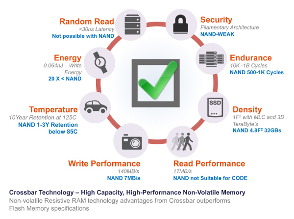
Stealth startup Crossbar’s RRAM technology will deliver 20x faster write performance; 20x lower power consumption and 10x the endurance at half the die size, compared to today’s best-in-class NAND Flash memory. Since it is CMOS-compatible, it can be easily integrated into existing fabs and processes without any special equipment or materials.
RRAM, ReRAM all refer to what HP calls memristors.
According to market research firm Webfeet Research, non-volatile memory is expected to grow to become a $48.4 billion market in 2016. Crossbar plans to bring to market standalone chip solutions, optimized for both code and data storage, used in place of traditional NOR and NAND Flash memory. Crossbar also plans to license its technology to system on a chip (SOC) developers for integration into next-generation SOCs.
This new generation of non-volatile memory will be capable of storing up to one terabyte (TB) of data on a single 200mm2 chip, enabling massive amounts of information, such as 250 hours of HD movies, to be stored and played back from an IC smaller than a postage stamp. Crossbar today also announced it has developed a working Crossbar memory array at a commercial fab, a major milestone in the development of new memory technology, signaling its readiness to begin the first phase of productization.
Samsung has stackable Flash competitor to memristors
-Samsung Electronics Co., Ltd., the world leader in advanced memory technology, today announced that it has begun mass producing the industry’s first three-dimensional (3D) Vertical NAND (V-NAND) flash memory, which breaks through the current scaling limit for existing NAND flash technology. Achieving gains in performance and area ratio, the new 3D V-NAND will be used for a wide range of consumer electronics and enterprise applications, including embedded NAND storage and solid state drives (SSDs).
Samsung’s new V-NAND offers a 128 gigabit (Gb) density in a single chip, utilizing the company’s proprietary vertical cell structure based on 3D Charge Trap Flash (CTF) technology and vertical interconnect process technology to link the 3D cell array. By applying both of these technologies, Samsung’s 3D V-NAND is able to provide over twice the scaling of 20nm-class* planar NAND flash.
The memory is based on a charge-trap cell rather than the conventional floating gate non-volatile cell used in 2D NAND flash. In the vertical arrangement this charge-trap cell shows increased reliability between a factor of 2 and a factor of 10 over conventional floating-gate NAND flash memory, Samsung claimed in a press release.
The technology is capable of stacking up 24 layers, but Samsung did not disclose how many layers it had used in its 128 Gbit vertical NAND, nor whether the memory cells are multilevel cell or whether it had relaxed the design geometry from the leading edge in 2D memory, which stands at about 19 or 16 nm.
If you liked this article, please give it a quick review on ycombinator or StumbleUpon. Thanks

Brian Wang is a Futurist Thought Leader and a popular Science blogger with 1 million readers per month. His blog Nextbigfuture.com is ranked #1 Science News Blog. It covers many disruptive technology and trends including Space, Robotics, Artificial Intelligence, Medicine, Anti-aging Biotechnology, and Nanotechnology.
Known for identifying cutting edge technologies, he is currently a Co-Founder of a startup and fundraiser for high potential early-stage companies. He is the Head of Research for Allocations for deep technology investments and an Angel Investor at Space Angels.
A frequent speaker at corporations, he has been a TEDx speaker, a Singularity University speaker and guest at numerous interviews for radio and podcasts. He is open to public speaking and advising engagements.
