

My Android phone is literally several billion times more powerful, per dollar, than the computer I used when I was a student. And it’s also 100,000 times smaller. We’ll do both of those things again in 25 years. It’ll be a billion times more powerful, and will be the size of a blood cell.
Based upon past reviews by Ray of his own predictions, Ray Kurzweil intends for his predictions to be accurate to the decade. This means blood cell sized supercomputers can happen anytime from 2033-2044 and Kurzweil would consider it to be correct. Ray could even say plus ten years around the 2038 date and anytime before (2014-2048). The implication and context of Ray’s prediction is that these blood cell sized supercomputers would be as common as Android cellphones and as affordable. However, the number of units is implied, so having a one off example that cost millions of dollars might still qualify.

How could various technological developments fulfill a petaflop of computing power in a blood cell?
It would definitely need to be precisely constructed to the nanometer in a 3D volume.
A red blood cells has roughly 7800 X 7800 X 2500 cubic nanometers. 152 billion cubic nanometers or 152 cubic microns.
Memristors can be formed from the intersection of nanowires that are about 2.5 nanometers thick. Memristors can form memory and compute elements. HP is trying to create nanostore architectures which would be memristors with memory and computing together. Assuming 3D crossbar computing could be created and operated and cooled at full density then this would enable perhaps 1 billion 3D crossbar elements. They are also trying to develop memristors with photonic communication. If they elements were massively parallel and operating at megahertz frequencies then they would produce 1 petaflop. A million parallel elements operating at a gigahertz would also achieve a petaflop.

IBM is trying to develop combined power and cooling with liquid batteries to enable petaflop computers in a 10 liter volume within 10-15 years. This would reduce it from the current size of a basketball court. This would be about 1 million times smaller. A further million times reduction in volume would be 10 microliters in say 20-30 years from today. A microliter is 1 billion cubic microns. Getting to red blood cell volume would be another reduction of about 100 million times.
I think pushing more regular technology to the limit could achieve a petaflop in a computing volume the size of a red blood cell but getting the full system with power and cooling into that volume would be a problem.
Single Atom Qubit Quantum Computers from Michelle Simmons and Room Temperature Quantum dots from Wolkow
These single atom devices would seem to require molecular nanotechnology to properly scale and build.
The smallest transistor ever built – in fact, the smallest transistor that can be built was created using a single phosphorous atom by an international team of researchers at the University of New South Wales, Purdue University, the University of Melbourne and the University of Sydney.
A controllable transistor engineered from a single phosphorus atom has been developed by researchers at the University of New South Wales, Purdue University and the University of Melbourne. The atom, shown here in the center of an image from a computer model, sits in a channel in a silicon crystal. The atomic-sized transistor and wires might allow researchers to control gated qubits of information in future quantum computers. (Purdue University image)
The technical meat of the TedX video is about 12 minutes into this 16 minute video

Although single atoms serving as transistors have been observed before, this is the first time a single-atom transistor has been controllably engineered with atomic precision. The structure even has markers that allow researchers to attach contacts and apply a voltage, says Martin Fuechsle, a researcher at the University of New South Wales and lead author on the journal paper.
“The thing that is unique about what we have done is that we have, with atomic precision, positioned this individual atom within our device,” Fuechsle says.
Simmons says this control is the key step in making a single-atom device. “By achieving the placement of a single atom, we have, at the same time, developed a technique that will allow us to be able to place several of these single-atom devices towards the goal of a developing a scalable system.”
The single-atom transistor could lead the way to building a quantum computer that works by controlling the electrons and thereby the quantum information, or qubits. Some scientists, however, have doubts that such a device can ever be built.
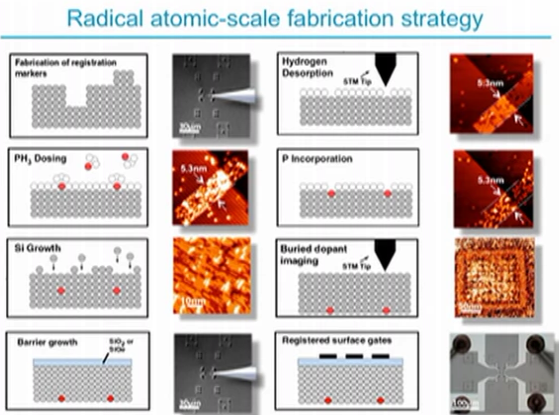
They embedded a wire in crystalline silicon to isolate the dopant atoms from surfaces and interfaces that caused this deactivation. They predicted this would give us highly conductive wires, and this is what happened.
The key to making these wires was combining scanning tunneling microscopy, a technique to image and manipulate individual atoms, with molecular beam epitaxy, a way of growing perfect crystals. It gave us great precision in all three dimensions, and when combined with a high density of the dopant atoms, allowed us to create these highly conductive nanowires.
Nature Nanotechnology – A single-atom transistor
a, Perspective STM image of the device, in which the hydrogen-desorbed regions defining source (S) and drain (D) leads and two gates (G1, G2) appear raised due to the increased tunnelling current through the silicon dangling bond states that were created. Upon subsequent dosing with phosphine, these regions form highly phosphorus-doped co-planar transport electrodes of monatomic height, which are registered to a single phosphorus atom in the centre of the device. Several atomic steps running across the Si(100) surface are also visible. b, Close-up of the inner device area (dashed box in a), where the central bright protrusion is the silicon atom, which is ejected when a single phosphorus atom incorporates into the surface. c, Schematic of the chemical reaction to deterministically incorporate a single phosphorus atom into the surface. Saturation dosing of a three-dimer patch (I) at room temperature (RT) followed by annealing to 350 °C allows successive dissociation of PH3 (II–IV) and subsequent incorporation of a single phosphorus atom in the surface layer, ejecting a silicon adatom in the process (V).
Robert Wolkow room temperature quantum dots and Quantum Cellular Automata
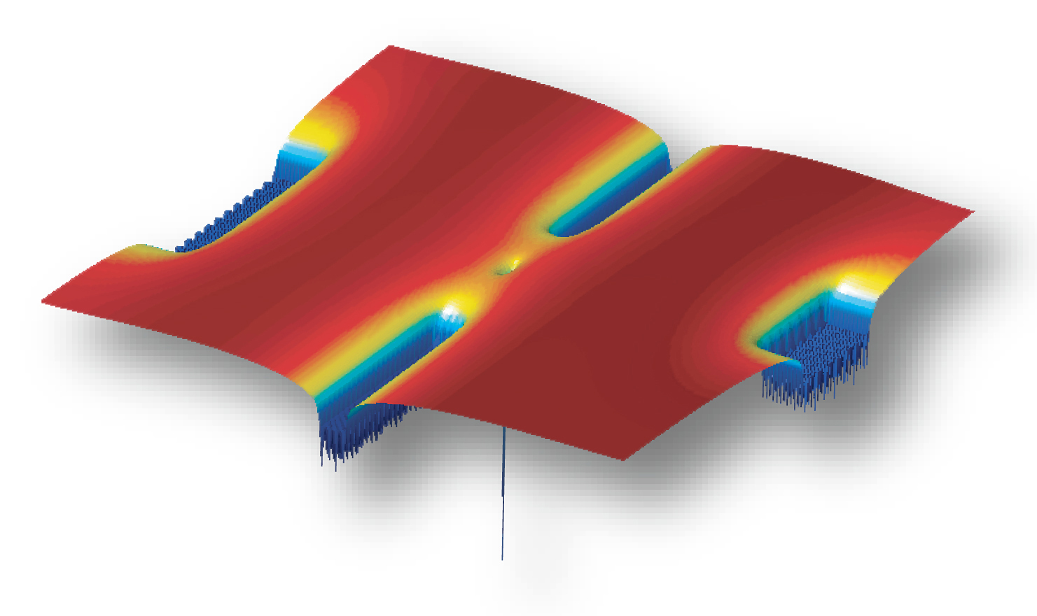
Four atomic quantum dots are coupled to form a “cell” for containing electrons. The cell is filled with just two electrons. Control charges are placed along a diagonal to direct the two electrons to reside at just two of the four quantum dots comprising the cell. This new level of control of electrons points to new computation schemes that require extremely low power to operate. Such a device is expected to require about 1,000 times less power and will be about 1,000 times smaller than today’s transistors.

Four dangling bonds that trap two electrons.
We report for the first time an experimentally observable tunnel coupling between zero-dimensional entities of atomic size: Si atom dangling bonds (DB) on an otherwise hydrogen terminated silicon crystal surface. Such DBs can serve as quantum dots and due to their strong charge localization, circumvent key problems associated with QD charging. Indeed, we show here that the charging and the tunnel coupling behavior within DB assemblies can be controlled even at room temperature. In addition, due to the fundamental similarities with semiconductor QDs and to the common Si-based fabrication platform, our approach can bring important advances to many of the above applications.
The robustness of the atomic system described here results from the relatively great energy level spacing of bound states. For this same reason, the coupling and controlled electron filling of assemblies of coupled DBs is achieved at room temperature rather than requiring cryogenic conditions. We assert that such DB states hold the prospect of a novel route to advancement in nano-electronics and computing devices, offering extreme miniaturization and a well-understood route to fabrication.
FURTHER READING
Robert Wolkow page
Quantum dot cellular automaton at wikipedia
A proposal for implementing classical cellular automata by systems designed with quantum dots has been proposed under the name “quantum cellular automata” by Paul Tougaw and Craig Lent, as a replacement for classical computation using CMOS technology. In order to better differentiate between this proposal and models of cellular automata which perform quantum computation, many authors working on this subject now refer to this as a quantum dot cellular automaton.
Complementary metal-oxide semiconductor (CMOS) technology has been the industry standard for implementing Very Large Scale Integrated (VLSI) devices for the last two decades, and for very good reasons – mainly due to the consequences of miniaturization of such devices (i.e. increasing switching speeds, increasing complexity and decreasing power consumption). Quantum Cellular Automata (QCA) is only one of the many alternative technologies proposed as a replacement solution to the fundamental limits CMOS technology will impose in the years to come.
Although QCA solves most of the limitations CMOS technology, it also brings its own. Optimistic assumptions suggest that intrinsic switching time of a QCA cell is in the order of terahertz, however, as mentioned earlier, switching speed is not limited by a cell’s intrinsic switching speed but by the proper quasi-adiabatic clock switching frequency setting. “Comparative analysis of circuit performance of QCA and CMOS against a representative computer task, suggests that realistic circuits of solid state QCA will have the maximum operating frequency of several megahertz. Small circuits of hypothetical molecular QCA might have the maximum operating frequency of several GHz, however, as the circuit size increases, capacitive loading effects will reduce the speed.” Moreover, solid-state QCA devices cannot operate at room temperature [until this new work]. The only alternative to this temperature limitation is the recently proposed “Molecular QCA” which theoretically has an inter-dot distance of 2 nm and an inter-cell distance of 6 nm. Molecular QCA is also considered to be the only feasible implementation method for mass production of QCA devices. QCA technology resolves, in principle, the problems of current CMOS technology, and it is only limited by the availability of its practical fabrication methods.
If you liked this article, please give it a quick review on ycombinator or StumbleUpon. Thanks

Brian Wang is a Futurist Thought Leader and a popular Science blogger with 1 million readers per month. His blog Nextbigfuture.com is ranked #1 Science News Blog. It covers many disruptive technology and trends including Space, Robotics, Artificial Intelligence, Medicine, Anti-aging Biotechnology, and Nanotechnology.
Known for identifying cutting edge technologies, he is currently a Co-Founder of a startup and fundraiser for high potential early-stage companies. He is the Head of Research for Allocations for deep technology investments and an Angel Investor at Space Angels.
A frequent speaker at corporations, he has been a TEDx speaker, a Singularity University speaker and guest at numerous interviews for radio and podcasts. He is open to public speaking and advising engagements.