

The U.S. Naval Research Laboratory (NRL), Materials Science and Technology Division, has taken delivery of a state-of-the-art Cameca 4000X Si Local Electrode Atom Probe (LEAP), a high performance microscope that provides precise atom-by-atom dissection of a material volume, enabling true three-dimensional (3D) atomic-scale reconstructions of material microstructures.
“Exact knowledge of where individual atoms are in a material is of tremendous benefit when engineering new materials,” said Keith Knipling, NRL Materials Science and Technology Division. “We expect the LEAP to greatly enhance our capability to develop new materials, including the next generation of structural alloys for stronger ship hulls and more advanced turbine engines, new electronic materials for tomorrow’s faster integrated circuits, and advanced solar cell and battery materials with improved power and energy efficiency.”
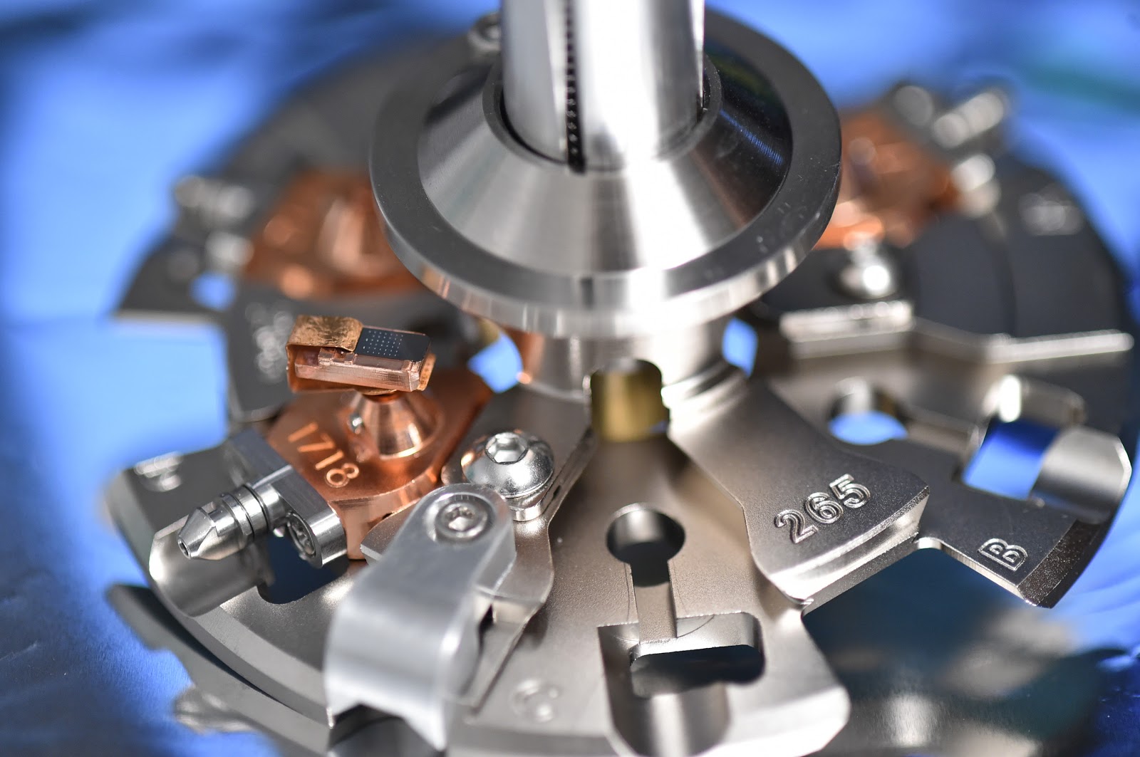
Researchers at the U.S. Naval Research Laboratory, Washington, D.C., are utilizing a state-of-the-art Cameca 4000X Si Local Electrode Atom Probe (LEAP) that provides nano-scale surface, bulk, and interfacial materials analysis of simple and complex structures. Microtip arrays are placed into copper pucks (shown labeled 1718) and then loaded onto carousels that are then placed in the instrument for analysis. Material experiments rely on the principle of field evaporation, whereby a strong electric field is applied to the sharply pointed specimen sufficient to cause removal of atoms by ionization.
(Photo: U.S. Naval Research Laboratory/Jamie Hartman)

The U.S. Naval Research Laboratory, Washington, D.C., has taken delivery of the only Local Electrode Atom Probe (LEAP) microscope in use in the U.S. Department of Defense (DoD). Researchers at the laboratory’s Materials Science and Technology Division will utilize the atom probe to analyze materials at the atomic level for optimizing new, next-generation alloys and semiconducting materials. (Photo: U.S. Naval Research Laboratory/Jamie Hartman)
The LEAP works using the principle of field evaporation, whereby a strong electric field applied to a needle-like specimen is sufficient to cause removal of atoms by ionization. Atom evaporation is triggered either by a voltage or laser pulse applied to the sample. The resulting ions are accelerated away from the specimen and identified chemically by time-of-flight mass spectrometry and their positions are deduced from the coordinates of ion impacts on a position-sensitive detector. By repeating this sequence, the atoms are progressively removed from the tip, and a 3D image of the material can be reconstructed at the atomic scale.
“Mapping the location of each chemical species in a material microstructure enables an unprecedented understanding of the true effects of alloying and material synthesis, which is essential for truly optimizing the properties of any material. We expect the LEAP to deliver new atomic-scale perspective and insights into a wide range of materials science investigations. For example, researchers at NRL are developing semiconductor materials with very dilute levels of added ‘dopant’ atoms for the purpose of tailoring their electrical properties,” Knipling adds. “These doped materials form the building blocks of nearly all semiconductor electronic devices such as diodes, transistors, solar cells, LEDs, and integrated circuits.
Most analytical techniques are incapable of measuring these small concentration levels, much less where the dopants segregate within the microstructure. With the LEAP, researchers can now answer these questions.”
Worldwide, there are only a handful of LEAP microscopes in use. NRL Materials Science and Technology Division possesses the only one in use by the U.S. Department of Defense (DoD)

Brian Wang is a Futurist Thought Leader and a popular Science blogger with 1 million readers per month. His blog Nextbigfuture.com is ranked #1 Science News Blog. It covers many disruptive technology and trends including Space, Robotics, Artificial Intelligence, Medicine, Anti-aging Biotechnology, and Nanotechnology.
Known for identifying cutting edge technologies, he is currently a Co-Founder of a startup and fundraiser for high potential early-stage companies. He is the Head of Research for Allocations for deep technology investments and an Angel Investor at Space Angels.
A frequent speaker at corporations, he has been a TEDx speaker, a Singularity University speaker and guest at numerous interviews for radio and podcasts. He is open to public speaking and advising engagements.