
“A single microprocessor has a billion transistors in it,” said Northwestern Engineering’s Mark Hersam. “All billion of them work. And not only do they work, but they work reliably for years or even decades.”
When trying to make the leap from an individual, nanotube-based transistor to wafer-scale integrated circuits, many research teams, including Hersam’s, have met challenges. For one, the process is incredibly expensive, often requiring billion-dollar cleanrooms to keep the delicate nano-sized components safe from the potentially damaging effects of air, water, and dust. Researchers have also struggled to create a carbon nanotube-based integrated circuit in which the transistors are spatially uniform across the material, which is needed for the overall system to work.
Now Hersam and his team have found a key to solving all these issues. The secret lies in newly developed encapsulation layers that protect carbon nanotubes from environmental degradation.

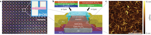
Complementary SWCNT TFT structures.
“One of the realities of a nanomaterial, such as a carbon nanotube, is that essentially all of its atoms are on the surface,” said Hersam, the Walter P. Murphy Professor of Materials Science and Engineering. “So anything that touches the surface of these materials can influence their properties. If we made a series of transistors and left them out in the air, water and oxygen would stick to the surface of the nanotubes, degrading them over time. We thought that adding a protective encapsulation layer could arrest this degradation process to achieve substantially longer lifetimes.”
Hersam compares his solution to one currently used for organic light-emitting diodes (LEDs), which experienced similar problems after they were first realized. Many people assumed that organic LEDs would have no future because they degraded in air. After researchers developed an encapsulation layer for the material, organic LEDs are now used in many commercial applications, including displays for smartphones, car radios, televisions, and digital cameras. Made from polymers and inorganic oxides, Hersam’s encapsulation layer is based on the same idea but tailored for carbon nanotubes.
To demonstrate proof of concept, Hersam developed nanotube-based static random-access memory (SRAM) circuits. SRAM is a key component of all microprocessors, often making up as much as 85 percent of the transistors in the central-processing unit in a common computer. To create the encapsulated carbon nanotubes, the team first deposited the carbon nanotubes from a solution previously developed in Hersam’s lab. Then they coated the tubes with their encapsulation layers.
Using the encapsulated carbon nanotubes, Hersam’s team successfully designed and fabricated arrays of working SRAM circuits. Not only did the encapsulation layers protect the sensitive device from the environment, but they improved spatial uniformity among individual transistors across the wafer. While Hersam’s integrated circuits demonstrated a long lifetime, transistors that were deposited from the same solution but not coated degraded within hours.
“After we’ve made the devices, we can leave them out in air with no further precautions,” Hersam said. “We don’t need to put them in a vacuum chamber or controlled environment. Other researchers have made similar devices but immediately had to put them in a vacuum chamber or inert environment to keep them stable. That’s obviously not going to work in a real-world situation.”
Hersam imagines that his solution-processed, air-stable SRAM could be used in emerging technologies. Flexible carbon nanotube-based transistors could replace rigid silicon to enable wearable electronics. The cheaper manufacturing method also opens doors for smart cards — credit cards embedded with personal information to reduce the likelihood of fraud.
“Smart cards are only realistic if they can be realized using extremely low-cost manufacturing,” he said. “Because our solution-processed carbon nanotubes are compatible with scalable and inexpensive printing methods, our results could enable smart cards and related printed electronics applications.”
Abstract
Over the past two decades, extensive research on single-walled carbon nanotubes (SWCNTs) has elucidated their many extraordinary properties making them one of the most promising candidates for solution-processable, high-performance integrated circuits. In particular, advances in the enrichment of high-purity semiconducting SWCNTs have enabled recent circuit demonstrations including synchronous digital logic, flexible electronics and high-frequency applications. However, due to the stringent requirements of the transistors used in complementary metal–oxide–semiconductor (CMOS) logic as well as the absence of sufficiently stable and spatially homogeneous SWCNT thin-film transistors the development of large-scale SWCNT CMOS integrated circuits has been limited in both complexity and functionality. Here, we demonstrate the stable and uniform electronic performance of complementary p-type and n-type SWCNT thin-film transistors by controlling adsorbed atmospheric dopants and incorporating robust encapsulation layers. Based on these complementary SWCNT thin-film transistors, we simulate, design and fabricate arrays of low-power static random access memory circuits, achieving large-scale integration for the first time based on solution-processed semiconductors.

Brian Wang is a Futurist Thought Leader and a popular Science blogger with 1 million readers per month. His blog Nextbigfuture.com is ranked #1 Science News Blog. It covers many disruptive technology and trends including Space, Robotics, Artificial Intelligence, Medicine, Anti-aging Biotechnology, and Nanotechnology.
Known for identifying cutting edge technologies, he is currently a Co-Founder of a startup and fundraiser for high potential early-stage companies. He is the Head of Research for Allocations for deep technology investments and an Angel Investor at Space Angels.
A frequent speaker at corporations, he has been a TEDx speaker, a Singularity University speaker and guest at numerous interviews for radio and podcasts. He is open to public speaking and advising engagements.