

Scientists at Rice, with support from Los Alamos National Laboratory, have made inch-wide films of densely packed, chirality-enriched single-walled carbon nanotubes
In the right solution of nanotubes and under the right conditions, the tubes assemble themselves by the millions into long rows that are aligned better than once thought possible, the researchers reported.
The thin films offer possibilities for making flexible electronic and photonic (light-manipulating) devices, said Rice physicist Junichiro Kono, whose lab led the study. Think of a bendable computer chip, rather than a brittle silicon one, and the potential becomes clear, he said.
“Once we have centimeter-sized crystals consisting of single-chirality nanotubes, that’s it,” Kono said. “That’s the holy grail for this field. For the last 20 years, people have been looking for this.”
The Rice lab is closing in, he said, but the films reported in the current paper are “chirality-enriched” rather than single-chirality. A carbon nanotube is a cylinder of graphene, with its atoms arranged in hexagons. How the hexagons are turned sets the tube’s chirality, and that determines its electronic properties. Some are semiconducting like silicon, and others are metallic conductors.
A film of perfectly aligned, single-chirality nanotubes would have specific electronic properties. Controlling the chirality would allow for tunable films, Kono said, but nanotubes grow in batches of random types.
For now, the Rice researchers use a simple process developed at the National Institute of Standards and Technology to separate nanotubes by chirality. While not perfect, it was good enough to let the researchers make enriched films with nanotubes of different types and diameters and then make terahertz polarizers and electronic transistors.
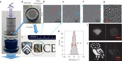
Fabrication and characterization of wafer-scale monodomain films of aligned CNT
The Rice lab discovered the filtration technique in late 2013 when graduate students and lead authors Xiaowei He and Weilu Gao inadvertently added a bit too much water to a nanotube-surfactant suspension before feeding it through a filter assisted by vacuum. (Surfactants keep nanotubes in a solution from clumping.)
The film that formed on the paper filter bore further investigation. “Weilu checked the film with a scanning electron microscope and saw something strange,” He said. Rather than drop randomly onto the paper like pickup sticks, the nanotubes – millions of them – had come together in tight, aligned rows.
“That first picture gave us a clue we might have something totally different,” He said. A year and more than 100 films later, the students and their colleagues had refined their technique to make nanotube wafers up to an inch wide (limited only by the size of their equipment) and of any thickness, from a few to hundreds of nanometers.
Further experiments revealed that each element mattered: the type of filter paper, the vacuum pressure and the concentration of nanotubes and surfactant. Nanotubes of any chirality and diameter worked, but each required adjustments to the other elements to optimize the alignment.
The films can be separated from the paper and washed and dried for use, the researchers said.
They suspect multiwalled carbon nanotubes and non-carbon nanotubes like boron nitride would work as well.
Co-author Wade Adams, a senior faculty fellow at Rice who specializes in polymer science, said the discovery is a step forward in a long quest for aligned structures.
“They formed what is called a monodomain in liquid crystal technology, in which all the rigid molecules line up in the same direction,” Adams said. “It’s astonishing. (The late Rice Nobel laureate) Rick Smalley and I worked very hard for years to make a single crystal of nanotubes, but these students have actually done it in a way neither of us ever imagined.”
Why do the nanotubes line up? Kono said the team is still investigating the mechanics of nucleation — that is, how the first few nanotubes on the paper come together. “We think the nanotubes fall randomly at first, but they can still slide around on the paper,” he said. “Van der Waals force brings them together, and they naturally seek their lowest-energy state, which is in alignment.” Because the nanotubes vary in length, the researchers suspect the overhangs force other tubes to line up as they join the array.
The researchers found their completed films could be patterned with standard lithography techniques. That’s yet another plus for manufacturers, said Kono, who started hearing buzz about the discovery months before the paper’s release.
“I gave an invited talk about our work at a carbon nanotube conference, and many people are already trying to reproduce our results,” he said. “I got so much enthusiastic response right after my talk. Everybody asked for the recipe.”
Abstract
The one-dimensional character of electrons, phonons and excitons in individual single-walled carbon nanotubes leads to extremely anisotropic electronic, thermal and optical properties. However, despite significant efforts to develop ways to produce large-scale architectures of aligned nanotubes, macroscopic manifestations of such properties remain limited. Here, we show that large (over cm2) monodomain films of aligned single-walled carbon nanotubes can be prepared using slow vacuum filtration. The produced films are globally aligned within ±1.5° (a nematic order parameter of ∼1) and are highly packed, containing 1 million nanotubes in a cross-sectional area of 1 μm2. The method works for nanotubes synthesized by various methods, and film thickness is controllable from a few nanometres to ∼100 nm. We use the approach to create ideal polarizers in the terahertz frequency range and, by combining the method with recently developed sorting techniques, highly aligned and chirality-enriched nanotube thin-film devices. Semiconductor-enriched devices exhibit polarized light emission and polarization-dependent photocurrent, as well as anisotropic conductivities and transistor action with high on / off ratios.
SOURCES- Rice University, Nature Nanotechnology, Youtube

Brian Wang is a Futurist Thought Leader and a popular Science blogger with 1 million readers per month. His blog Nextbigfuture.com is ranked #1 Science News Blog. It covers many disruptive technology and trends including Space, Robotics, Artificial Intelligence, Medicine, Anti-aging Biotechnology, and Nanotechnology.
Known for identifying cutting edge technologies, he is currently a Co-Founder of a startup and fundraiser for high potential early-stage companies. He is the Head of Research for Allocations for deep technology investments and an Angel Investor at Space Angels.
A frequent speaker at corporations, he has been a TEDx speaker, a Singularity University speaker and guest at numerous interviews for radio and podcasts. He is open to public speaking and advising engagements.
