

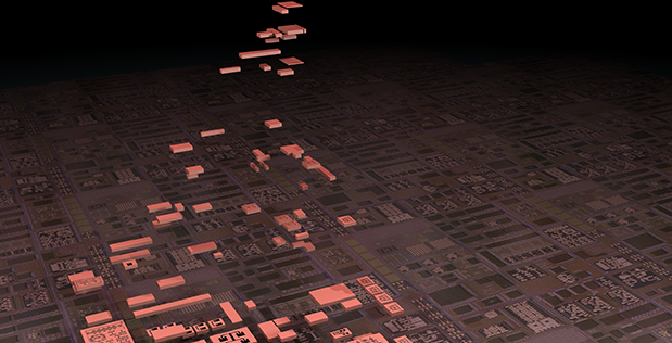
Open the hood of just about any electronic gadget and you probably will find printed circuit boards (PCBs)—most often in a leaf-green color—studded with processing, memory, data-relaying, graphics, and other types of chips and components, all interconnected with a labyrinth of finely embossed wiring. By challenging the technology community to integrate the collective functions hosted by an entire PCB onto a device approaching the size of a single chip, DARPA’s newest program is making a bid to usher in a fresh dimension of technology miniaturization.
“We are trying to push the massive amount of integration you typically get on a printed circuit board down into an even more compact format,” said Dr. Daniel Green, manager of the new program, whose acronym, “CHIPS,” is itself a typographic feat of miniaturization; the program’s full name is the Common Heterogeneous Integration and Intellectual Property (IP) Reuse Strategies Program. “It’s not just a fun acronym,” Green said. “The program is all about devising a physical library of component chips, or chiplets, that we can assemble in a modular fashion.”
A primary driver of CHIPS is to develop a novel, industry-friendly architectural strategy for designing and building new generations of microsystems in which the time and energy it takes to move signals—that is, data—between chips is reduced by factors of tens or even hundreds. “This is increasingly important for the data-intensive processing that we have to do as the data sets we are dealing with get bigger and bigger,” Green said. Although the program does not specify applications, the new architectural strategy at the program’s heart could open new routes to computational efficiencies required for such feats as identifying objects and actions in real-time video feeds, real-time language translation, and coordinating motion on-the-fly among swarms of fast-moving unmanned aerial vehicles (UAVs).
The CHIPS program is pushing for a new microsystem architecture based on the mixing and matching of small, single-function chiplets into chip-sized systems as capable of an entire printed circuit board’s worth of chips and components.
DARPA has posted a Request for Information (RFI), designated on fbo.gov as DARPA-SN-16-50, to harvest ideas at the front-end of the program from expert and industry players so that the CHIPS team can hone the details of the program in ways that would facilitate graceful incorporation of these new approaches within existing commercial semiconductor foundries and electronics fabrication facilities. “Key to the success of CHIPS will be standards and interfaces, and this means we will be working with a community, not all by ourselves,” said Green. The CHIPS team expects to use input from the RFI and a workshop anticipated to occur later this summer to prepare a Broad Agency Announcement (BAA). The BAA, which will also be posted on fbo.gov, will specify the program’s technical goals and how potential performers can submit proposals.
A major aspect of the CHIPS vision is the eventual availability of a library of custom and commercial “chiplets”—small-scale chips that individually embody a particular function, such as data storage, computation, signal processing, and managing the form and flow of data. By assembling and integrating dozens of chiplets, mosaic style, on a so-called interposer, which is like a printed circuit board writ small, all of those microsystems’ functions could be performed in a much closer huddle and can perform more efficiently than if they were distributed in the usual way among a suite of chips attached to a conventional PCB.
Another big win Green hopes to score with the modular architecture championed by the CHIPS program is the ability to separate out onto individual chiplets the many IP blocks developed for and aggregated into commercial monolithic chips. Such partitioning of computational functions could open the way for the DoD to negotiate more affordable licensing of smaller and more specific IP blocks suitable for repurposing for particular technologies and systems. “If CHIPS is successful, we will gain access to a wider variety of specialized IP blocks that we will be able to integrate into our systems more easily and with lower costs,” said Green. “This should be a win for both the commercial and defense sectors.”
Combine high performance ASIC characteristics with PCB like assembly
One technique for addressing rising cost and complexity has been the use of a modular design flow that subdivides a system into functional circuit blocks, called IP blocks. In this document, IP block refers to intellectual property captured in a pre-designed functional circuit block. Examples of IP blocks include, but are not limited to, timing circuits, filters, waveform generators, embedded processors, data converters, amplifiers, fast Fourier transforms (FFTs), serializer-deserializers (SERDES), and memory.
To fully realize the benefits of modular design, designers must be able to use IP blocks from various technologies and nodes. Printed circuit boards (PCBs) exemplify a platform for this type of heterogeneous assembly of IP blocks that can be completed rapidly and at low cost. However, the PCB approach has several disadvantages that limit their usefulness for DoD applications. For example, the distances between IP blocks are too large to be compatible with tomorrow’s highspeed requirements. Another problem is that signals must travel through layers of packaging to reach the die, incurring significant signal loss.
DARPA is interested in a new design strategy that can combine the high performance characteristics of ASICs with the rapid, low-cost, and heterogeneous assembly of PCBs. One possible path is to instantiate IP blocks as chiplets (functional dies) that can be assembled onto modular integration platforms. These chiplets would leverage standard layouts and interfaces to seamlessly link to other chiplets. This design methodology will hereafter be described as the CHIPS process. It is anticipated that the use of standard interfaces will enable access to a large catalog of commercial and government off-the-shelf (COTS/GOTS) IP blocks, reuse of existing IP blocks, and heterogeneous integration of blocks in other technologies and nodes. It is further anticipated that a fully implemented CHIPS ecosystem will substantially reduce the time and cost to realize new circuit functions.
To enable modular assembly of chiplets as described above, a common set of standard interfaces should be agreed upon. Multiple standards could exist depending on the range of targeted chiplets, however a minimum number of standards is imperative to encourage broad use. These standard interfaces should properly describe requirements across multiple layers, such as physical, electrical, control, software, etc. Requirements for documentation practices, so that designers can easily incorporate chiplets from multiple sources, are also of interest.
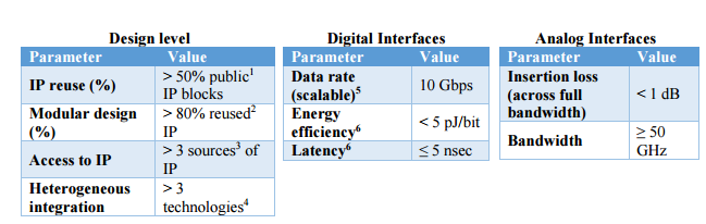
DARPA seeks innovative insights on how standard interfaces and IP reuse can be leveraged to create custom circuits in a fraction of today’s time and cost, with conventional methods for both digital and analog systems. To this end, DARPA is interested in discussions on the optimal set of design requirements that would motivate use of ‘CHIPS-like’ die-level integration in future electronic systems. Note that the interface and modularity requirements for digital and analog blocks are anticipated to diverge due to their dramatically different drivers. An example of a possible set of design metrics is listed in the table below.
SOURCES – DARPA, Common Heterogeneous Integration and IP Reuse Strategies (CHIPS) Request for Information (RFI)

Brian Wang is a Futurist Thought Leader and a popular Science blogger with 1 million readers per month. His blog Nextbigfuture.com is ranked #1 Science News Blog. It covers many disruptive technology and trends including Space, Robotics, Artificial Intelligence, Medicine, Anti-aging Biotechnology, and Nanotechnology.
Known for identifying cutting edge technologies, he is currently a Co-Founder of a startup and fundraiser for high potential early-stage companies. He is the Head of Research for Allocations for deep technology investments and an Angel Investor at Space Angels.
A frequent speaker at corporations, he has been a TEDx speaker, a Singularity University speaker and guest at numerous interviews for radio and podcasts. He is open to public speaking and advising engagements.