

Engineers at MIT have invented a fast, precise printing process that may make such electronic surfaces an inexpensive reality. In a paper published today in Science Advances, the researchers report that they have fabricated a stamp made from forests of carbon nanotubes that is able to print electronic inks onto rigid and flexible surfaces.
A. John Hart, the Mitsui Career Development Associate Professor in Contemporary Technology and Mechanical Engineering at MIT, says the team’s stamping process should be able to print transistors small enough to control individual pixels in high-resolution displays and touchscreens. The new printing technique may also offer a relatively cheap, fast way to manufacture electronic surfaces for as-yet-unknown applications.
“There is a huge need for printing of electronic devices that are extremely inexpensive but provide simple computations and interactive functions,” Hart says. “Our new printing process is an enabling technology for high-performance, fully printed electronics, including transistors, optically functional surfaces, and ubiquitous sensors.”
The key to printing tiny, precise, high-resolution patterns is in the amount of pressure applied to stamp the ink. The team developed a model to predict the amount of force necessary to stamp an even layer of ink onto a substrate, given the roughness of both the stamp and the substrate, and the concentration of nanoparticles in the ink.
To scale up the process, Mariappan built a printing machine, including a motorized roller, and attached to it various flexible substrates. The researchers fixed each stamp onto a platform attached to a spring, which they used to control the force used to press the stamp against the substrate.
“This would be a continuous industrial process, where you would have a stamp, and a roller on which you’d have a substrate you want to print on, like a spool of plastic film or specialized paper for electronics,” Hart says. “We found, limited by the motor we used in the printing system, we could print at 200 millimeters per second, continuously, which is already competitive with the rates of industrial printing technologies. This, combined with a tenfold improvement in the printing resolution that we demonstrated, is encouraging.”
After stamping ink patterns of various designs, the team tested the printed patterns’ electrical conductivity. After annealing, or heating, the designs after stamping — a common step in activating electronic features — the printed patterns were indeed highly conductive, and could serve, for example, as high-performance transparent electrodes.
Going forward, Hart and his team plan to pursue the possibility of fully printed electronics.
“Another exciting next step is the integration of our printing technologies with 2-D materials, such as graphene, which together could enable new, ultrathin electronic and energy conversion devices,” Hart says.
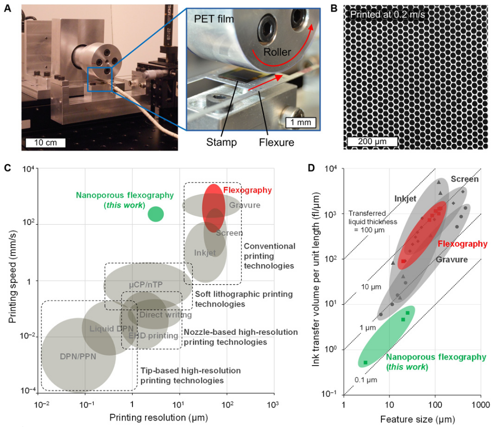
High-speed printing and process performance metrics.(A) Custom-built desktop P2R printing system with a CNT stamp attached on a flat flexure and a PET film attached to a roller with a diameter of 5 cm. (B) Optical microscope image of Ag honeycomb pattern with minimum internal linewidth of 3 μm printed on a PET substrate at a printing speed of 0.2 m/s using the P2R system. (C) Comparison of speed and resolution of conventional printing technologies for electronically functional materials. Conventional processes include flexography, gravure, screen, and inkjet. Soft lithography includes μCP and nTP; Nozzle-based high-resolution printing methods include direct writing and EHD printing. Tip-based methods include DPN and polymer pen lithography (PPN). (D) Comparison of volume per unit length, lateral feature size, and thickness of ink that transfers to the substrate by single print (by mechanical contact or drop) in conventional printing technologies, compared to nanoporous flexographic printing, as shown in this paper.

Direct printing of ultrathin colloidal ink patterns using microstructured nanoporous stamps.Schematics of the printing procedure (A) and the uniform transfer of ink (B) from the nanoporous stamp to the target substrate surface via conformal contact. (C) Scanning electrode microscopy (SEM) images of stamp features comprising an array of squares (side length, 25 μm), along with corresponding optical and atomic force microscopy (AFM) images of the resulting printed Ag ink [particle size, less than 10 nm; 50 to 60 weight % (wt %) in tetradecane] patterns. (D) Photographs of printed Ag ink patterns on a rigid glass plate and on a flexible polyethylene terephthalate (PET) film. (E) SEM image of the stamp feature (upper left) and optical microscope image of the printed Ag NP ink pattern (lower right) of a flower-like pattern with feature widths varying from 20 to 150 μm. (F) Fluorescence microscope image (wavelength emission, 620 nm) of printed QD ink (CdSe/ZnS, ~5 to 6 nm, 10 wt % dispersed in tetradecane) of a pattern with minimum internal linewidth of 5 μm and hole size of 11 μm.
Science Advances – Ultrathin high-resolution flexographic printing using nanoporous stamps
Since its invention in ancient times, relief printing, commonly called flexography, has been used to mass-produce artifacts ranging from decorative graphics to printed media. Now, higher-resolution flexography is essential to manufacturing low-cost, large-area printed electronics. However, because of contact-mediated liquid instabilities and spreading, the resolution of flexographic printing using elastomeric stamps is limited to tens of micrometers. We introduce engineered nanoporous microstructures, comprising polymer-coated aligned carbon nanotubes (CNTs), as a next-generation stamp material. We design and engineer the highly porous microstructures to be wetted by colloidal inks and to transfer a thin layer to a target substrate upon brief contact. We demonstrate printing of diverse micrometer-scale patterns of a variety of functional nanoparticle inks, including Ag, ZnO, WO3, and CdSe/ZnS, onto both rigid and compliant substrates. The printed patterns have highly uniform nanoscale thickness (5 to 50 nm) and match the stamp features with high fidelity (edge roughness, ~0.2 μm). We derive conditions for uniform printing based on nanoscale contact mechanics, characterize printed Ag lines and transparent conductors, and achieve continuous printing at a speed of 0.2 m/s. The latter represents a combination of resolution and throughput that far surpasses industrial printing technologies

Brian Wang is a Futurist Thought Leader and a popular Science blogger with 1 million readers per month. His blog Nextbigfuture.com is ranked #1 Science News Blog. It covers many disruptive technology and trends including Space, Robotics, Artificial Intelligence, Medicine, Anti-aging Biotechnology, and Nanotechnology.
Known for identifying cutting edge technologies, he is currently a Co-Founder of a startup and fundraiser for high potential early-stage companies. He is the Head of Research for Allocations for deep technology investments and an Angel Investor at Space Angels.
A frequent speaker at corporations, he has been a TEDx speaker, a Singularity University speaker and guest at numerous interviews for radio and podcasts. He is open to public speaking and advising engagements.