

At the 2016 IEEE International Electron Devices Meeting (IEDM) in San Francisco, researchers from CEA-Leti presented two papers unveiling promising nanowire architectural blocks for the 5 nanometer node.
This Nanowire Surface Potential (NSP) based model, they write, was validated both by numerical simulations and experimental data, which leads us to the second paper, “Vertically Stacked-Nanowires MOSFETs in a Replacement Metal Gate Process with Inner Spacer and SiGe Source/Drain,” demonstrating an actual physical implementation.
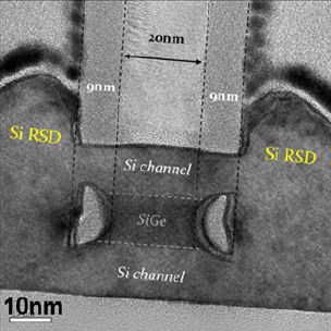
In this paper, Leti shares its finding on the very first functional devices featuring stacked-NWs transistors with integrated inner spacers to reduce parasitic capacitances and SiGe source drain (S/D) stressors to boost performance.
Both building blocks are required for the 5nm node, the researchers believe, which would extend the scaling limits of CMOS technology as a natural progression from FinFETs.
In this work, a predictive and physical compact model for NanoWire/NanoSheet (NW/NS) Gate-All- Around (GAA) MOSFET is presented. Based on a novel methodology for the calculation of the surface potential including quantum confinement, this model is able to handle arbitrary NW/NS cross-section shape of stacked-planar and vertical GAA MOSFETs (circular, square, rectangular). This Nanowire Surface Potential (NSP) based model, validated both by numerical simulations and experimental data, is demonstrated to be very accurate in all operation regimes of GAA MOSFETs.

Brian Wang is a Futurist Thought Leader and a popular Science blogger with 1 million readers per month. His blog Nextbigfuture.com is ranked #1 Science News Blog. It covers many disruptive technology and trends including Space, Robotics, Artificial Intelligence, Medicine, Anti-aging Biotechnology, and Nanotechnology.
Known for identifying cutting edge technologies, he is currently a Co-Founder of a startup and fundraiser for high potential early-stage companies. He is the Head of Research for Allocations for deep technology investments and an Angel Investor at Space Angels.
A frequent speaker at corporations, he has been a TEDx speaker, a Singularity University speaker and guest at numerous interviews for radio and podcasts. He is open to public speaking and advising engagements.